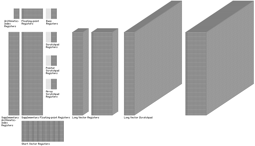
The computer described here has the following complement of registers which may potentially be directly visible to the ordinary programmer:
where a register is like the display on a pocket calculator; a place where a number is kept with which the computer is currently working.
Eight registers are Arithmetic/Index Registers. They are used for calculations on 32-bit integers, as well as calculations on shorter 16-bit or 8-bit integers. Also, the number in one of these registers can be used by an instruction as an index register; that means the number will indicate which element of an array is to be used for a calculation.
Eight registers are Base Registers. While addresses in this computer are 32 bits long, to allow a large amount of memory to be used, it would be wasteful to include a 32-bit address in every instruction that refers to memory. Instead, instructions that refer to memory give the number of a Base Register, and its 32-bit contents are added to the 16-bit address in the instruction itself to identify the memory location to be used.
Note that the contents of an index register or a base register are both added to the address in an instruction, but they are normally used for opposite purposes. The base register indicates the large area of memory being used; the address in the instruction indicates the particular variable being used; and the index register indicates the element of an array variable.
A base register ordinarily points to an area of memory that is 65,536 bytes in size. In short page mode, the size of that area is reduced to 4,096 bytes, so that address fields in instructions are shorter. This allows the base register field in an instruction to be shifted to the 16-bit halfwords added to the instruction for addresses, allowing for more possible opcodes.
Additional registers in the diagram above which are only applicable in some of the computer's possible modes of operation. The scratchpad, scratchpad pointer, and array scratchpad registers are used to point to small areas of memory, which permit 16-bit instructions to perform operations referencing this area of memory in the scratchpad modes; in the normal mode, only a register to register operation takes only 16 bits, and all memory references take at least 32 bits. The short vector registers are available in the normal mode of operation, but not in some others, and provide a way for the computer to operate on several numbers at once. The supplementary registers are available in vector register mode (and symmetric vector register mode and multi-way vector register mode) and, in addition to providing a fast register bank, are also used when the computer operates on a larger group of numbers at once.
Also, there are eight integer long vector registers, each one the size of the entire array of 64 supplementary arithmetic/index registers, and eight floating point long vector registers, each one the size of the entire array of 64 supplementary floating-point registers, and there are also two long vector scratchpads, an integer one and a floating point one, each containing 64 registers similar to the eight registers in the banks of long vector registers.
The diagram only shows the registers normally used for arithmetic. The computer also has a program counter and a program status block, these are not shown in the diagram. In addition, there are registers only used within the execution of an Execute Extended Translate instruction; since they are only used inside an instruction, they need not be considered as part of the program state.
Also not shown in the diagram above are the explicit bit matrix multiply registers, as it is considered that these are only allocated to programs in special circumstances, and the area where programs used in an Execute Extended Translate instruction, and defined by a Define Extended Translate instruction, are stored; this area, while at least some part of it is envisaged as operating at register speeds rather than even cache speeds on a typical full implementation, still is treated or behaves, at least for Code 0 programs, more like memory than registers, and its size and organization can vary.
The following diagram:
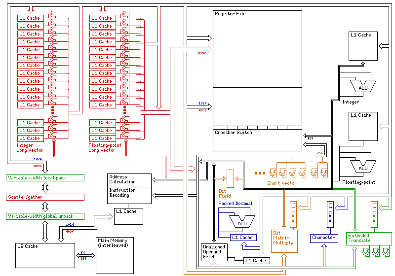
indicates how a high-performance implementation of this architecture might work. This shows sets of sixty-four ALUs, all operating in parallel, for performing long vector operations. Because the operands of long vector instructions can be of different sizes, this creates some complexity in how data paths would be structured.
As well, if the portions of the diagram shown in red are removed, with the width of one data path (which is also the width of the Level 2 cache) changed from that in red to that in blue, this diagram also serves to show the general layout of a more realistic implementation, comparable to existing microprocessors, but lacking the ability to use the cache-internal parallel computing feature, and the ability to use long vector instructions within the sequence established by a Compose Pipeline Sequence instruction, but otherwise implementing the complete instruction set.
Green shows specialized functions of the architecture that are largely peculiar to it, the ability to emulate variable-width memory and the extended operate function; orange shows features historically found on specialized computers such as bit field operations and bit matrix multiply, and also includes one, the short vector unit, that has now become a part of the standard instruction repertoire on most computers; deep blue character and decimal manipulation instructions, which, while an optional part of the System/360 architecture, tend to be left out of most computers today.
Historically, while computers like the Lincoln Laboratories TX-2, with operations similar to the short vector instructions, used multiple ALUs in parallel, machines such as the Cray-1 with instructions analogous to the long vector instructions implemented them by pipelining a single arithmetic unit. Thus, realistic implementations of this architecture might do likewise; in that case, the cache-internal parallel computing feature would, of course, be unavailable.
Although a realistic implementation of the architecture might not have a full 64 ALUs for performing long vector operations, it is also intended that long vector instructions are to be preferred over short vector instructions as the most efficient means of performing vector operations.
This can be dealt with by providing more than one conventional ALU so that some degree of superscalar operation is provided.
Even if a maximum-performance implementation is chosen, 128-bit floating point is a luxury feature that could well be omitted from the arithmetic-logic units making up a large set, whether of 64 of them or 16 of them. Note that a bank of arithmetic-logic units capable of operating on 16 double-precision floating-point numbers at once would match the performance of the CELL processor from IBM and Toshiba, with eight subsidiary cores operating on 128-bit vectors, which can be used to contain two 64-bit floating-point numbers, and so at least that level of performance is realizable with current technology.
Omitting 128-bit arithmetic from most of the available floating-point ALUs would also affect, when an alternate word length is selected, 96-bit, 80-bit, and even 72-bit floating-point arithmetic as well. While this might be regretted, it is also true that the ability to vary the word size for data provided in this architecture is also a luxury feature, being, in fact, the one feature, of all the unusual features included with the architecture, that is likely unique to it.
There are also ways of performing more rapid multiplication or division that do not lend themselves well to the kind of partitioning that takes place in the short vector unit. At the cost of many additional gates, they allow the answer to a multiplication or division to be obtained in fewer cycles. But they do not improve throughput; a slower arithmetic unit requiring fewer gates can still provide a net throughput of one multiplication or one division per cycle, just with a longer pipeline. Since an operation on a long vector is inherently parallel, that the main ALU might produce results in fewer clock cycles than the short vector ALU would not change its performance on vector operations relative to that of the short vector unit.
The diagram, however, shows the partitioning issue avoided through brute force, by simply providing a separate ALU for each precision provided.
The flow of control signals is omitted for simplicity, and features such as memory mapping are not dealt with at all. (As noted below, some additional discussion of related topics are present in this section; the next section discusses the related topic of instruction issue in detail.) Register renaming is not dealt with to any great extent in this diagram, but note that the register bank consists of dual-port memory; one path allows all 64 registers of the scratchpad registers or within a single vector register or vector scratchpad location to be transferred to the appropriate set of 64 parallel ALUs, the other path allows register banks belonging to different processes to be accessed independently, and then routed, through a crossbar switch, to the appropriate computational unit. Thus, what appears as the 128-bit and 256-bit wide data buses in the diagram include in addition multiple direct paths between the individual computational units and this crossbar switch.
Note that it appears that it would not be possible to save on the amount of circuitry required by using a Beneš network here instead of a crossbar switch, as the routing of registers to functional units may change with each cycle, and requiring the instruction decoding unit to work out the correct switch settings for each required routing would add many cycles to the latency of all instruction execution. Even improved forms of that network, designed for more efficient control, such as the KR-Beneš network do not seem to be applicable.
A unit for fetching unaligned operands is used as part of the process of fetching bit fields, and is needed for packed decimal operands and floating-point numbers of type medium (since they are aligned on 16-bit boundaries but are longer than 16 bits, they may cross the boundaries of larger aligned areas).
An internal data bus 4,096 bits in width serves both integer long vector computations and the bit matrix multiply unit, allowing both to receive data quickly from the register file. The bus that brings data to and from the cache is a smaller, but still generous, 256 bits in width.
Another item not shown on the diagram is the unit applied to the 4,096 bit bus to perform the load transposed instruction, and the units on the 4,096, the 8,192, and the 256 bit wide buses for assisting with Fourier transforms, so even as an overview diagram, it is greatly simplified.
The following diagram:
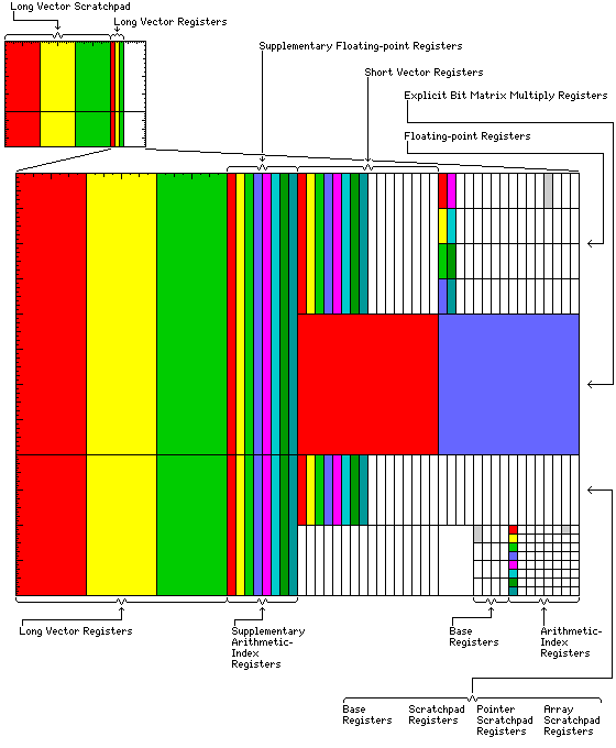
illustrates the way in which the register file shown in the diagram above may be allocated to different processes.
As this diagram shows exactly those registers as are visible to the programmer being allocated, it presupposes an in-order design. While this is not completely unreasonable, as another characteristic noted for this proposed processor is that it will be massively multithreaded, in general only RISC designs, rather than a CISC design such as this one, can be in-order without severely impacting performance. There is a discussion of the reasons for this on this page about another hypothetical architecture oriented towards high performance. Other approaches than providing extra spaces in each group of registers, however, are possible as ways of enabling out-of-order operation.
In the most urgent and basic case of allowing the retrieval of data from memory to be requested ahead of time, the memory management unit can contain buffer storage for data retrievals on the fly. To allow calculations to be interleaved that use the same register for different values, as it is noted that the L1 cache for each functional unit is intended to be made of the same kind of storage cells as used in the register file (as the cost of using six transistors instead of four seems to be well worth it) placing intermediate results there is not unreasonable; in fact, since the register file is a central and global resource, serving many threads and many functional units, instead of it being the highest level of storage, the register file may end up being effectively situated between L1 and L2 cache, at least for the floating-point registers and the arithmetic/index registers, and most likely the short vector registers as well. (Computations involving the long vector registers, while they might be overlapped, would not be treated in an out-of-order fashion; both because of the size of those registers, and because their inherent structure, in eliminating the need for loop constructs, achieves the same result in facilitating dense pipeline use as out-of-order operation without additional assistance.) A page is now available which attempts to explain out-of-order execution. |
A register file large enough to allow more than one process to run using all the features of the architecture is shown; it contains 256 rows, each one containing one 8,192-bit segment corresponding in size to an entire set of 64 supplementary floating-point registers, and one 4,096-bit segment corresponding in size to an entire set of 64 supplementary arithmetic/index registers. 8 such rows make a set of long vector registers, and 64 such rows make a long vector scratchpad.
Note that while this is a reasonable minimum size of register file for this type of architecture, it does involve 384 kilobytes of register (not cache) space, which reflects the fact that this architecture includes features in the supercomputer class.
Actually, 256 kilobytes would be sufficient, but dividing the register file into two parts, one part half the size of the other, makes the diagram simpler to label. It would mean that only at most two processes using the full long vector scratchpad registers, rather than three, could be running at one time.
Also, in practice, a register file allowing essentially unrestricted register renaming for the smaller register banks might not be used, since there is no practical reason to have thousands of processes running concurrently, and since the addressing involved could lead to circuit delays; thus, instead of one large register file as shown here, divided only into what can be roughly viewed as integer and floating-point parts, multiple specialized register files may be more likely.
Another reason for that is because of the need for an inter-register buffer to permit transfers of data between registers for register-to-register operations. The inter-register bus for the arithmetic/index registers should not conflict with the inter-register bus for the supplementary arithmetic/index registers, and so on.
In this diagram, three processes are allocated a full set of long vector scratchpad registers, and a full set of long vector registers. One of those processes, and a fourth process, is allocated a set of sixteen explicit bit matrix multiply registers.
The first eight processes have colors given to them in this diagram; all eight of these processes are allocated supplementary registers, and the forty-ninth process, the first of the last sixteen, which are only allocated the minimum set of registers essential for normal mode operation, is also given a color for clarity.
The first sixteen processes, including these eight, also have short vector registers; an additional thirty-two processes with only the arithmetic/index registers, the floating-point registers, and base registers accompanied by the various scratchpad registers can also be accomodated. A final sixteen processes are only allocated the standard base registers, and not the scratchpad registers, allowing a total of sixty-four processes to run.
As the requirements of the extended translate operations are variable, no attempt has been made to depict them in the diagram.
As for the Program Status Blocks for processes executing concurrently, the operating system would maintain these in memory, except for those of the processes actually running; how multiple processes can be successively issuing instructions that enter the pipeline is discussed to an extent in this section.
It is, of course, perfectly reasonable to omit the long vector registers and the long vector arithmetic-logic units; this still obtains a high-performance architecture with a host of mainframe features. The supplementary registers, since they can be used for other purposes besides holding a long vector, can usefully be retained in this case.
One could design a chip with a second processor core, but only one set of long vector arithmetic-logic units, and it could be designed so that in the event of chip flaws, the chip could be usable as a single-core processor, a processor with a reduced amount of cache, a processor lacking some of the more ambitious features of the design, such as the long vector capability, or even a co-processor for use in an external vector arithmetic unit. This sort of thing is, in fact, merely standard practice in microprocessor fabrication.
The on-chip cache in a full implementation of the architecture is envisaged as being eight megabytes in size.
This is a large size for a cache; at present, microprocessors with supercomputer-like instruction sets, might have what are considered very large caches which are two megabytes in size, although that has even more recently increased to six megabytes in one case.
The reason such a large L2 cache is needed is because of the very aggressively multithreaded architecture of the chip; with many processes running concurrently (or, in fact, simultaneously) each one needs an adequate amount of cache. Could the fact that different parts of the cache belong to different processes be exploited to reduce the requirement for actual cache memory?
I believe that one possibility is suggested by U. S. Patent 5,867,443, issued in 1999 to Dr. Richard W. Linderman, working at the Rome Air Development Center.
Machines which used bulk core in their memory hierarchy, as opposed to drum memory, as secondary storage appear wasteful, in a way, since the random access feature of the bulk core is not fully used, as only block transfers take place between it and main memory.
The output from a magnetic core that indicates if it contains a 1 or a 0 is very weak, and it required amplifier circuitry much more expensive and bulky than one core to make it useful as a logic input. The outputs from the transistors used in semiconductor RAM are not quite so weak.
Let us consider a memory that contains a grid of cells, each containing perhaps one, or four, or sixteen bits of fast static RAM used for cache, and perhaps 64 or 256 bits of slower dynamic RAM. In addition to functioning as a static RAM, it would be capable, in the cycle time of the dynamic RAM, to transfer a bit from one of the bits of the dynamic RAM to one of the bits of the static RAM, or one bit in the other direction, in every one of the cells in this memory.
Thus, one can think of such a memory conceptually as looking like this:
although, in practice, something like this would be a more practical layout:
Having such a wide bandwidth for moving large chunks of data in and out of the fast memory from the slow memory would, it seems, allow such a combined memory to more closely resemble a fast memory with the capacity of the slow memory than a conventional cache made from fast memory, connected to a slow memory by a bus, simulates a fast memory with the capacity of that slow memory.
Hence, this closer simulation of a large fast memory could serve as a cache to an external slow memory, providing the less close simulation of an even larger fast memory. That is, the slow memory on the chip, which is overlaid by the fast memory, would, by virtue of its very high-bandwidth connection to the fast memory, add to the effective capacity of that fast memory as a cache, being able to serve it as the slow memory external to the chip could not. Having a second port into this memory for direct transfers to the slow memory is likely to be useful.
The abstract principle shown here, however, may not be too useful, as current dynamic RAM memory cells do, in fact, normally have a sufficiently low output that they do indeed require column amplifiers. But if we use a larger cell size, perhaps with 1,024 bits of dynamic RAM in each cell, the overhead of putting 32 column amplifiers in each cell would not, perhaps, be excessive, and the larger cell size need not impair the transfer bandwidth, since one could also put more static RAM bits in each cell, and transfer 32 bits within a cell at the same time.
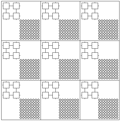
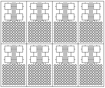
This leads to a cache memory organized in bit-planes having the arrangement shown below:
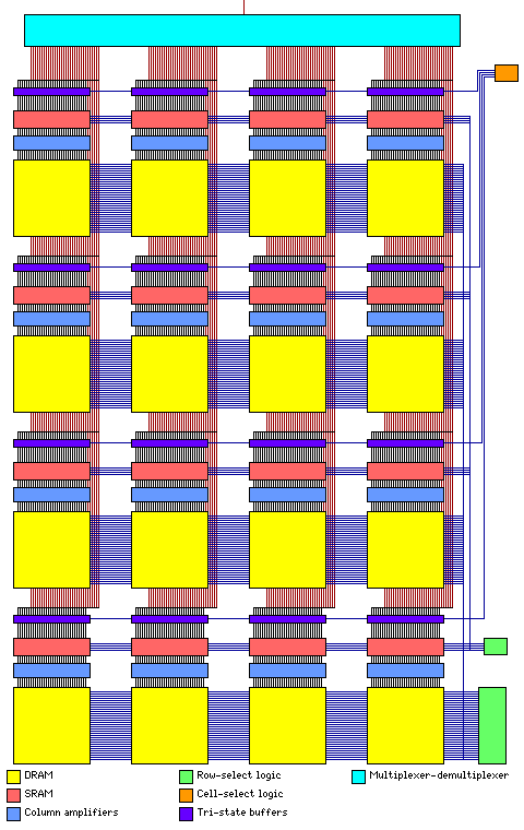
Of course, there would be many such bit planes, so that more than one bit is transferred out at a time, but the multiplexer/demultiplexer on square arrays is still needed, along with the row-select logic, to facilitate addressing a large number of words. On the other hand, one could just use more row-select logic (or, in terms of the system as shown in this diagram, cell-select logic) instead, making the array a long and thin rectangle instead, and that probably is the more common practice with semiconductor RAM.
Also, note that since 32 bits, rather than 1 bit, are being transferred with a cell, there is no longer multiplexer/demultiplexer logic within the cells, so the cells aren't really separated from one another in any meaningful way in the horizontal direction in the diagram any longer. This design is very similar to Virtual Channel Memory, as developed by NEC; only subtle differences exist, in that the memory is now very rich in buffers, and therefore the data transferred to the buffers in a single parallel operation, instead of being destined to be immediately transferred in a single burst from the memory to the processor, is largely to be simply kept in the buffers for future random references. Thus, the differences lie in the intended mode of use of the memory, and in changing the ratio of the kinds of memory cells to suit that mode of use. But, in addition, there is a significant difference: the size of the parallel transfer from the memory to the buffers is increased because the buffers are in small groups, and each small group of buffers is associated with its own portion of the total DRAM on the chip; the diagram is of the memory on a single chip, and is simplified to show a 4 by 4 matrix instead of, say, a 32 by 32 matrix, not of a system of chips.
To recap, the benefit of this design is that in each of the sixteen cells shown in the diagram, a transfer between the same word in the 32 words of DRAM, and the same word in the 4 words of SRAM, in the same cell, could take place in parallel. Thus, we have a memory divided into thirty-two pages, with four one-page "windows" that function at SRAM speeds, and which can be quickly moved from one page to another in the time of a single access to DRAM.
Another contemporary example of what I discuss above, even more closely similar, is the Renesas M32R microprocessor. This chip, designed for use in consumer products, includes on-chip dynamic RAM with a wide path to cache on the chip. The chip has a RISC architecture, and some models include 32-bit floating-point hardware. The only difference is that the on-chip DRAM is used as main memory, not as supplemental cache. IBM has used on-chip DRAM to supply L3 cache in some of its products, so I'm really discussing nothing new here.
The data path from the chip into main memory would be 256 bits wide, and the main memory is envisaged as being 16-way interleaved. Since information from main memory can be fetched in units of 4,096 bits, or 512 bytes, in that circumstance, the cache is thus to be organized as 16,384 cache lines, each 4,096 bits wide.
In addition to each cache line being labelled with the physical address of the main memory from which it was loaded, or to which it will be saved, each cache line can also be labelled with one address in the form (Process ID)/(Base Register Number)/(Displacement); since, normally, base register contents are infrequently changed, these labels will remain valid for a useful period of time, and will allow the addition of base register contents to the displacements in instructions, as well as the calculations involved in memory mapping, to be avoided for many instructions.
The data path from external memory into the cache will allow data from external memory to be placed, 256 bits at a time, along the length of each cache line.
For cache-internal parallel computing, as previously described, so that each of the 64 internal processors can have its memory mapped to a contiguous area of main memory, while still using the normal path between those processors and the cache, instead of allowing the main, or Level 2, cache to be split into 64-bit wide slices, the individual processors will each use their own Level 1 caches.
The data path from the cache to the vector ALU bank involves some complications. It is expected that these units can access successive bytes, halfwords, words, doublewords, and quadwords in cache. Thus, the data path from these arithmetic-logic units to the cache will vary in width from 512 bits to 8,192 bits in width.
In addition, although the computer normally operates with an eight-bit byte, it can also operate with a byte that is six, nine, or ten bits in width; with the six-bit byte, the number of bytes in floating-point types doubles; otherwise, the number of bytes in a type is usually unchanged. This is achieved by only partially filling the cache lines; those corresponding to the lowest-addressed locations are left empty, and of the sixteen 256-bit units in a cache line, twelve are used for a six-bit byte, ten for a ten-bit byte, and nine for a nine-bit byte. Suitably modified paths between cache memory and the vector ALU bank for data items from one to eight bytes in width (and also sixteen bytes in width for the six-bit byte only, as well as the normal eight-bit byte) are also required.
In addition to delivering data from the cache to the vector arithmetic-logic units, these paths would also serve to deliver data to the main 128-bit wide data bus of the chip for delivery to the main ALU.
One way in which this type of transformation can be achieved is illustrated in the overview diagrm above.
The Scatter/Gather unit is described on the page describing long-vector memory-reference instructions; when data is being fetched from the L2 cache, global scatter operations, followed by local gather operations, are used when individual elements of data are 32 bits, 16 bits, or 8 bits in width instead of 64 bits in width.
The Global Unpack unit globally, again, during a fetch from cache, treating the 4096-bit bus as containing a single string of bits, takes either the leftmost (or, possibly the rightmost, depending on the internal format of a partially-filled cache line; see the discussion concerning tagged word mode in the section about the Program Status Block for more concerning this topic) 512 6-bit characters, and places them in the least significant bits of the 512 8-bit bytes into which these 4096 bits are divided, or takes the leftmost 256 characters, either 9, 10, or 15 bits in width, and places them in the least significant bits of the 256 16-bit halfwords into which these 4096 bits are divided.
Thus, it is performing a global unpack operation.
The Local Pack unit, also during a fetch from cache, performs the inverse operation to that which the Global Unpack unit performs, except that it operates separately on each of the 64 64-bit doublewords into which the 4096 bits are divided, and except that in all cases it packs characters taken from those 64 bits into the rightmost bits of the 64 bit bus width.
Thus, this unit performs a local pack operation.
These units, and their placement, allows the global scatter and local gather operations within the Scatter/Gather unit that allow operands to have different widths for the standard memory organization to also work when a different memory width is chosen, so that the scatter/gather circuitry does not need to be duplicated with modifications for other memory widths.
The sequence of operations that are performed during a fetch from cache is, therefore:
and when information is stored in the cache from the registers or the arithmetic units, the reverse sequence that is performed is:
The following diagram may help to illustrate how the four phases work together, and why they must be ordered in the given sequence:
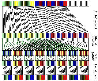
This diagram shows a scaled-down cache line, divided into eight blocks of 64 bits. Only six of these blocks are filled, and they are filled with packed 24-bit units of data. The global unpack step takes each packed 6-bit character, and places it in an 8-bit byte. The global scatter and local gather phases direct consecutive 32-bit words to consecutive arithmetic-logic units, and then the local pack phase turns a 32-bit word composed of 8-bit bytes each containing 6 bits of data into a 24-bit word suitable for performing arithmetic operations.
It should also be noted that the circuitry for interprocessor communications described here will need to operate on data after global unpack, but prior to global scatter, in order to align operands properly, and so a direct path to the arithmetic-logic units from this phase is required; since each of these four steps may be omitted, this should naturally exist in any case.
As the design being considered will be using a cache line consisting of sixteen blocks of 256 bits, but instead of having sixteen ALUs, there will be sixty-four ALUs, each 64 bits wide, it should be noted that the width of the local gather and local pack phases (and their inverses) is geared to the width of the ALU and not the block.
When memory is divided into 36-bit words, when the string character size is 6 bits, string characters are accessed by means of the circuitry used for a division of memory into 24-bit words. This principle applies to other word sizes and character sizes as well, and avoids a need to duplicate the circuitry for 6 bit characters, 9 bit characters, 10 bit characters, and 15 bit characters.
Operating on individual 6-bit or 10-bit characters in a 30-bit word, since the 40-bit word with natural 10-bit bytes uses 10 out of 16 spaces in a cache line, and a 24-bit word with natural 6-bit bytes uses 12 out of 16 spaces in a cache line, while a 30-bit word with natural 15-bit bytes uses 15 out of 16 spaces in a cache line, requires a loopback around these three units not shown in the diagram. No such situation arises with the 6-bit characters in a 36-bit word, since it uses 9 out of 16 spaces in a cache line, less than the 12 out of 16 spaces in a cache line used for the 24-bit word with natural 6-bit bytes.
Note that while in general the term byte is used synonymously with octet on these pages, referring always to a unit of 8 bits, the term byte is sometimes used with a different meaning which is still different from the meaning of the term character. There can be six characters, each six bits wide, in a 36-bit word. But the number of bytes in a word must always be a power of two; thus, for a 36-bit word, the character size may be six bits, but the byte size must be nine bits.
Note that areas of the cache can be reserved for the use of a specific process. In addition to reserving an area of the cache for conventional cache use by a high-priority process, and reserving an area of the cache for use with cache-internal parallel computing, up to three areas of the cache can be reserved for use as the primary main memory used by a process: one for use by means of the direct cache instruction modes, one for use by means of the full cache instruction modes, and one for use by means of the postfix supplementary bit which performs direct cache indication. It is necessary to allow three separate areas to be reserved in this way, since these three mechanisms of indicating cache use are independent of each other, although the modes necessary to use all three at once, full cache versions of the direct cache modes, are not currently included among those this architecture supports.
It is of course envisaged that the use of an error-correcting code with memory will be supported.
A subset of the [128,120,4] Hamming code can be used to allow one error to be corrected, and two errors to be detected, in 64 bits of data from memory with an overhead of one byte; this is the same level of overhead that would have been required merely to provide one bit of parity to every byte in memory.
Because there is a considerable amount of freedom in the design of a code with such properties, error-correcting codes of this type have been designed that have additional desirable properties.
One due to Mu-Yue Hsiao, for example, minimizes the probability that an error of three or more bits will produce a valid symbol. Another, due to Douglas C. Bossen, will correct an error in two bits, provided that they are adjacent. Both of these codes were devised at IBM. And another, due to Shigeo Kaneda at NTT, will detect an error in up to four bits, provided they are all in one of the four-bit nybbles into which the 72-bit input word can be evenly divided.
As described in U. S. Patent 5,490,155, held by Compaq (filed on October 2, 1992 and granted on February 6, 1996, and hence still in force), one can take an error-correcting code that deals with an n-bit wide failure, and increase that to 2n bits wide by interleaving such a code when 128 bits are fetched from memory. Thus, with a 256-bit bus to memory, four-way interleaving is possible.
Also, depending on what type of chip is used in a specific module, the optimal error-correcting code for use with that module would change; thus, memory modules should have, and perhaps do have, a means of indicating whether they contain, say, for one which provides a 72-bit wide memory word, nine 8-bit wide chips, eighteen 4-bit wide chips, or so on.
Also, the chip would be able to use only part of the data path so as to access I/O devices, including such things as memory in video cards; thus, the ability to be used in a system with memory that is only 128 bits wide or 64 bits wide (144 bits or 72 bits including ECC bits) and to reduce the interleaving of error correction would also be useful. As well, for memory widths lower than 64 bits, a fallback to byte parity would be appropriate.
It may be possible for a code to be either SEC-DED-S4ED or SEC-DED-S2EC depending on what action is taken in response to various syndromes, just as a code with a minimum Hamming distance of 4 can be used either to correct single errors and detect double errors, or to detect triple errors, however, avoiding the need to change between three different error-correcting codes. A code devised by Chin-Long Chen, also at IBM, is either a SEC-DED-S4ED code or a SEC-DED-S3ED code (since 72 is divisible by 3, chips which hold 3 bits could be used, since they were used for 30-pin error-correcting memory modules which provided 9 bits at each address) depending on how it is used, and so this provides an indication this might be possible. An S2EC code is included in, and therefore has less strict requirements as, the 2-adjacent code due to Douglas C. Bossen noted above.
However, if a code is designed as a (144,128) code instead of a (72,64) code, better properties can be achieved, and that is even more true of a (288,256) code; hence, interleaving is only a solution used in the absence of designing an ideal code for the specific application. It is possible to design a (144,128) code that corrects errors in one 4-bit block and detects errors in any two 4-bit blocks, and, starting from a Bose-Chaudhuri-Hocquenghem code, it is possible to design a (284,256) code that corrects errors in any three bits, and detects errors in any four bits, and so a (288,256) code has four extra bits available above those required for a TEC-QED code.
Also, it may be noted that by keeping track of errors observed, once it is known that a particular memory module has failed, an error-correcting code can then be decoded based on that knowledge, allowing a SEC-DED code to correct a second random error in addition to the error that is already known and expected.
The high-performance implementation of the architecture shown above has the ability to initiate sixty-five 64-bit floating-point division operations on every clock cycle. In general, normal programs will not make full use, or anything close to full use, of the potential power of the chip. However, there are instructions, such as the CPS (compose pipeline sequence) instruction that do provide a way for the programmer to use the chip's full power when the application can benefit thereby.
If a chip constantly produces a large amount of heat, then a cooling fluid at a very low temperature, such as liquid nitrogen, could be used to remove a large quantity of heat with a limited flow of liquid. But when the chip has a huge difference between its maximum and minimum heat output, use of a very cold cooling fluid risks causing low-temperature damage to the chip. One way to deal with this would be to use temperature sensors to regulate the amount of cooling performed at a given time; this has the limitation that response to changing conditions has to be sufficiently rapid to avoid damage from either too much heat or too much cold.
An alternative way to avoid problems in this type of situation would be to cool the chip with a very rapid flow of large quantities of chilled water. A sufficiently large flow would have the capacity to take away all the excess heat produced at full power, while the temperature of the fluid would not be low enough to cause damage to the chip even if it was not generating significant quantities of heat.
It may be noted that while the architecture described here is quite elaborate, it could of course be implemented in silicon by means of a microcoded implementation that kept most of the registers in external RAM.
A more efficient implementation is also approaching the bounds of possibility; based on some existing chips, I have estimated that it might be possible to fit it into a die size somewhere in the vicinity of 2000 square millimeters with an 0.13 micron process, and therefore on a realizable die size with a smaller process at some time in the near future. This architecture, however, includes many features which will only be useful to a very few prospective users. Thus, it is not one that would be considered for an actual implementation until it was not merely possible to implement, but instead when it was very easy to implement; when the number of gates available on a microchip is so large that designers would despair of finding useful things to do with them.
It may also be noted that some of the features of this architecture, such as its having not two, but four, endian modes, and being able to combine bisequential operation with extended translate mode, are wilfully bizarre; it is intended that the explanation of how such features work here would equip readers to understand actual historical computer architectures, some of which also had unusual features.