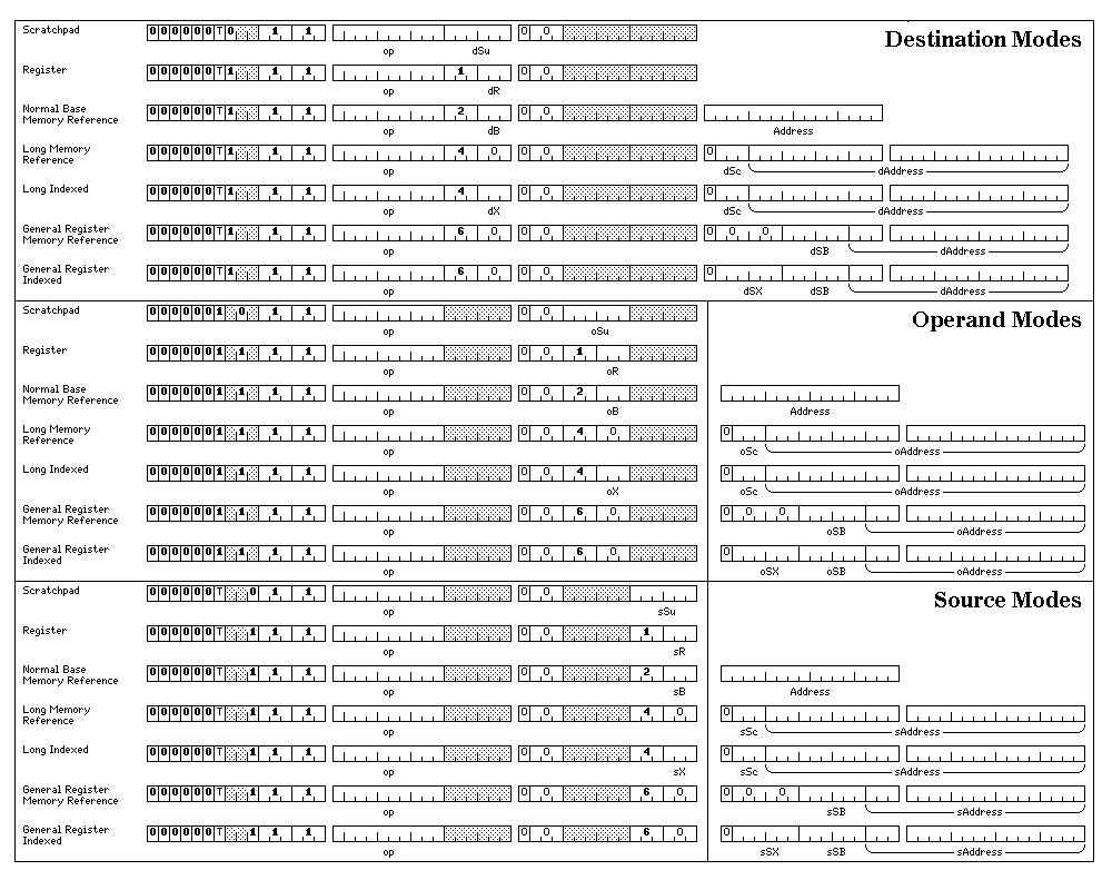
In addition to long vector instructions, a complete set of addressing modes which allow the use of the 64 supplementary registers for scalar instructions is provided. The possible modes are illustrated below in their three-address form:
with the addresses that may be required to be appended to the instruction for the operand argument being placed after those for the destination argument, and with those required for the source argument placed after those for the operand argument.
Next, they are illustrated below in their shorter two-address form:
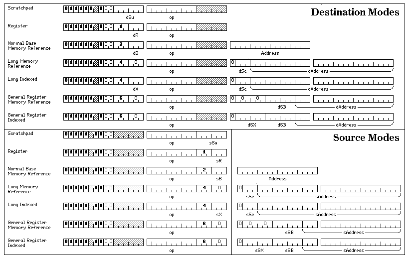
The short two-address form is available from Normal Mode, Scratchpad Mode and Condensed Mode. The three-address form is available from Normal Mode, Scratchpad Mode, Condensed Mode, Compact Mode, Local Mode and with modified opcodes from Simple Mode as well.
In Simple Mode, instructions that begin with:
1xxxxxx001001000
are equivalent to instructions beginning
0000xxxxxx001001
in Compact Mode, which is how the three-address long vector instructions and other related instructions are reached from that mode.
In Normal Mode, this class of instructions now begins with:
0100xxxxxx001001
due to recent design changes.
In addition to an addressing mode in which the eight scratchpad registers serve as base registers, pointing to areas of memory which may contain up to 268,435,456 bytes, having a 28-bit displacement, a mode is provided where the sixty-four supplementary registers are used both for the base register and the index register, and the displacement is 19 bits long, leading to each of these base registers indicating an area containing up to 524,288 bytes.
When the sixth bit, which is bit 5 when big-endian bit numbering is in use (and bit 10 when little-endian bit numbering is in use), of the first halfword is a one, we proceed to the long vector instructions, which are similar in format.
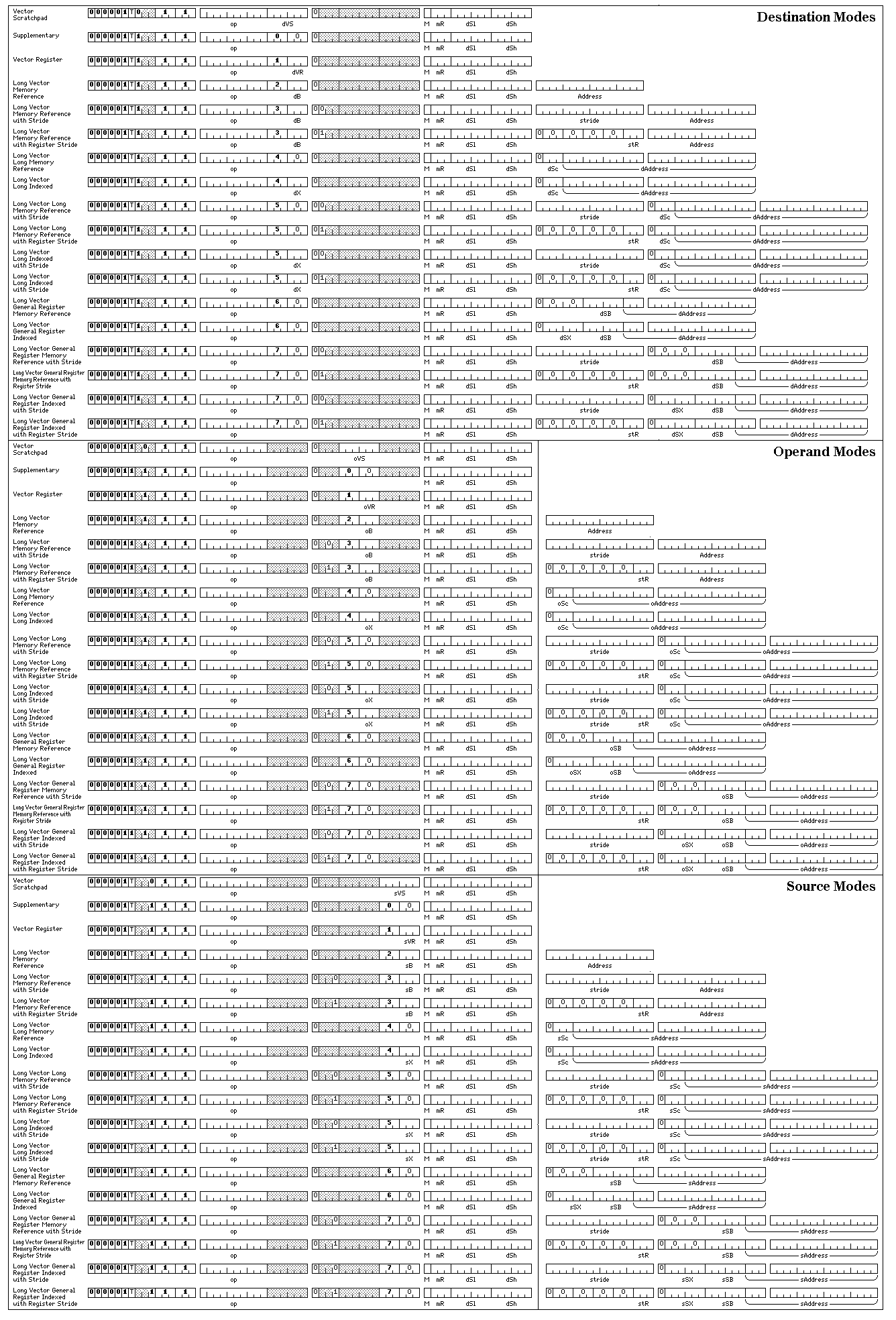
Only the three-address form is illustrated, although a two-address form similar to the shorter two-address form shown above also exists for these instructions (although not for the analogous instructions for short vector operands; instead, the two-address form is obtained by setting the bit marked T to zero in this longer format).
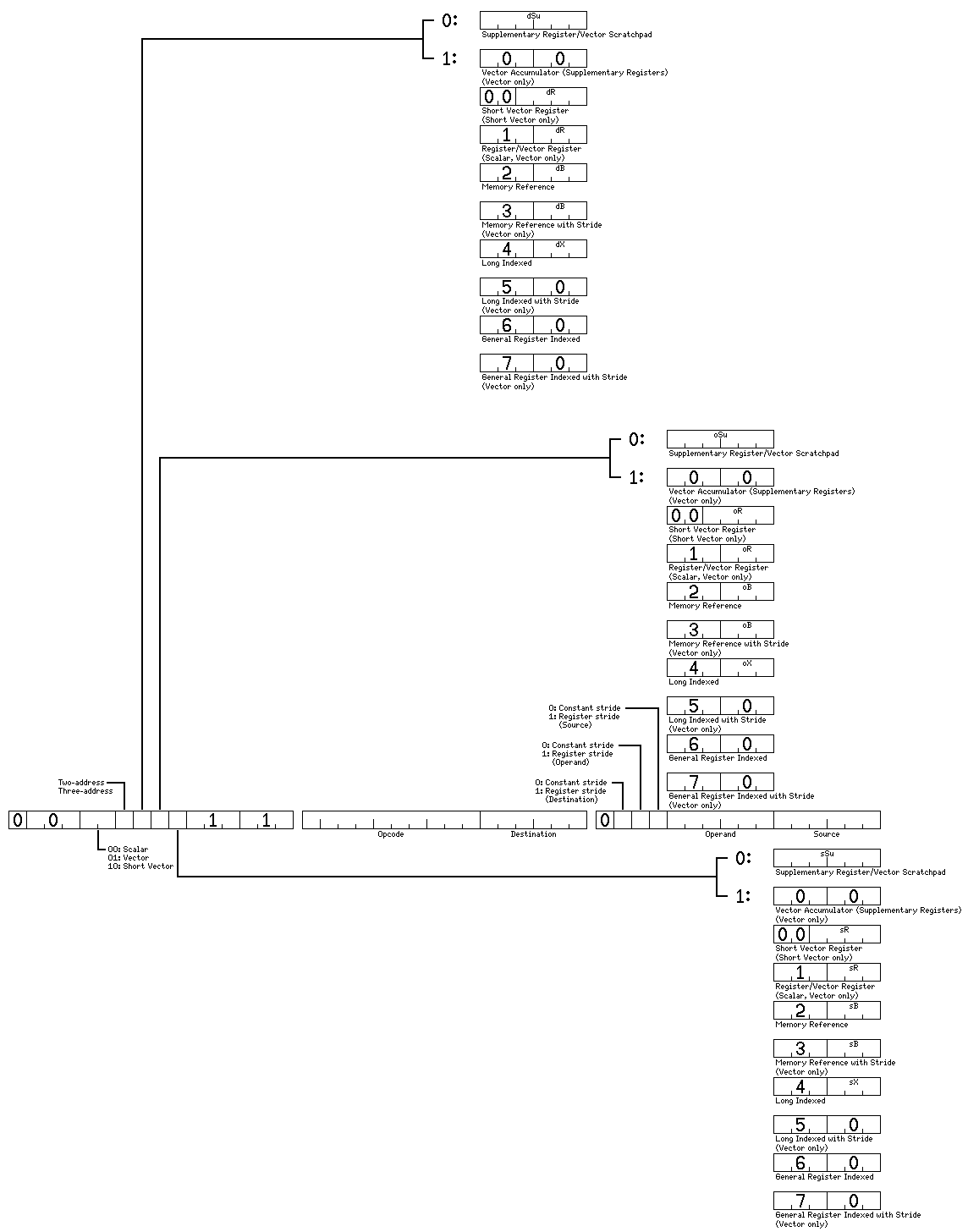
The intent is that three bits indicate if the source, operand and destination operands are supplementary registers, and, if they are not, the first three bits of the six-bit source or destination field indicates the addressing mode for that operand in an orthogonal manner, so that any of the addressing modes illustrated here in the most common combinations can be used for either the source or destination operands, allowing, for example, memory-to-memory instructions where both the source and destination operands are specified in the long indexed format.
How this works may be made clearer by the diagram below:
Note that this diagram also illustrates the addressing modes for the short vector instructions, which will be encountered on the next page.
The two-address vesions of these instructions are similarly illustrated by this diagram:
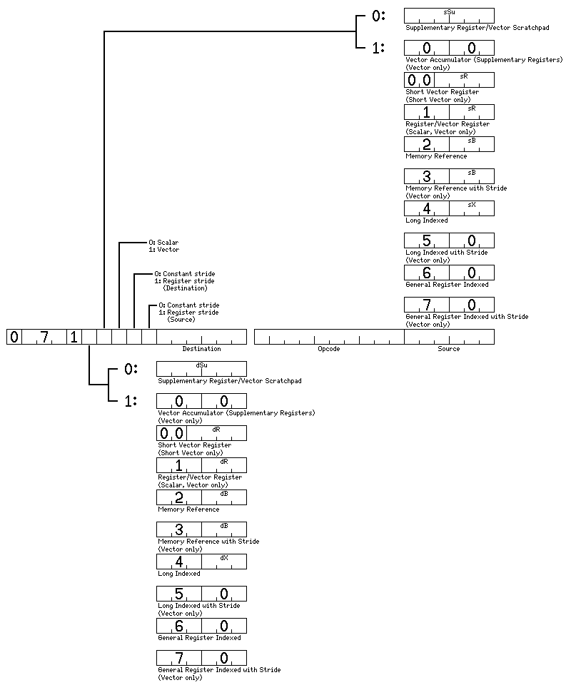
The vector instructions with nine-bit opcodes shown above all involve the vector registers, which contain only up to 64 items. Thus, they include a word indicating if a mask register is used, and also having two fields indicating the first and the last of the positions within the 64 elements of a 64 element vector register that are to be used.
The functions of some of the addressing modes illustrated in the diagrams above are:
Vector Scratchpad: in this instruction format, the source and the destination are both found among the sixty-four vector scratchpad registers.
Scratchpad to Vector Scratchpad: the source operand is the supplementary registers, and the destination operand is one of the sixty-four vector scratchpad registers.
Vector Register to Vector Scratchpad: the source operand is one of the eight vector registers, and the destination operand is one of the sixty-four vector scratchpad registers.
Long Vector Long Memory Reference: the source operand is one of the eight vector registers, and the destination operand is a vector in memory. This is a vector operation, and a range of the 64 elements in the vector scratchpad register used is indicated, together with an optional mask, if the M bit is one, found in the register indicated by the mR field. When a range is used to indicate a vector of less than 64 elements is used, while the starting and ending elements indicate which elements of the vector scratchpad register are used, the operand in memory is simply a vector of less than 64 elements which starts at the effective address. Elements of the vector that are to be ignored due to the use of the mask register, however, are in their assigned positions within the vector, which may begin with an ignored element, whether it is in a vector scratchpad register or in memory.
Long Vector Indexed: this is the indexed form of the Long Vector Long Memory Reference mode described above.
Long Vector Memory Reference: again, the source operand is one of the eight vector registers, and the destination operand is a vector in memory. Here, one of the Address/Base registers is used as the base register, and the displacement is 16 bits in length.
Long Vector Memory Reference with Stride represents a partial implementation of another feature found on Cray supercomputers.
The stride is a signed 16-bit field, giving the displacement between successive vector elements in memory. If the stride field contains a 1, the instruction is a conventional vector operation, thus, the displacement is in units of operand size, not bytes; if it is a zero, the memory operand is a scalar value.
The purpose of this is to facilitate matrix multiplications. Since a nonunit stride will lead to extra memory accesses in most implementations, the optimal way in which to perform matrix multiplication will be to load each column of the left matrix into the vector registers or vector scratchpad in turn, requiring an operation with nonunit stride, and then performing successive multiply and accumulate operations involving that operand in the register space with the rows of the right matrix, which is accessed using unit stride.
Note that the base register field may be zero, indicating Long Vector Long Memory Reference with Stride or Long Vector Indexed with Stride as well.
Note that the different possibilities for the source operand have been illustrated in the modes described above. The destination operand may also be varied between any of the types shown. Two examples to illustrate this are shown.
Vector Scratchpad to Vector Register: here, one of the sixty-four vector scratchpad registers is the source, and one of the eight vector registers is the destination.
Vector Register: this vector operation has one of the eight vector registers as its source and destination operands.
Because the sixty-four supplementary arithmetic/index registers are 64 bits long, rather than 32 bits long, in order that vector operations on the long type are possible, these additional opcodes:
0000101000   I     Insert
0000101010   UL    Unsigned Load
are defined for the vector addressing modes and those scalar addressing modes having a supplementary register as their destination register, controlling sign extension for loading a 32-bit value into a 64-bit register.
The short vector instructions are designed to be implemented by means of an arithmetic unit with a 256-bit wide register that can be partitioned into multiple areas, and in which all operations are carried out in parallel.
The long vector instructions, on the other hand, follow the principles used in computers where there is only a single conventional ALU, but which can still operate on several operands concurrently because it is pipelined. As a result, the Medium floating-point format is allowed with long vector instructions.
It is envisaged that the short vector arithmetic unit will be pipelined also, and, thus, in order that the long vector instructions, when available, will result in more arithmetic operations in a given time than the short vector instructions, it will be necessary to implement long vector operations with some degree of parallelism.
When parallelism is employed, special interconnections are required to permit the long vector arithmetic units to work not only on groups of consecutive double-precision floating-point numbers or consecutive long integers, which correspond to the most likely width of the data path between the long vector arithmetic units and the cache, but also on the same number of consecutive bytes, the same number of consecutive halfwords, the same number of consecutive integer or floating-point numbers, or, for that matter, the same number of consecutive extended (or quad) precision floating-point numbers.
Eight consecutive bytes, four consecutive 16-bit halfwords, and two consecutive 32-bit integers or floating-point numbers all occupy the same area in memory as one 64-bit double precision floating-point number or long integer, so circuitry is required to send them to consecutive arithmetic-logic units instead of to the same one.
The degree of parallelism provided can vary from one implementation to another. If complete parallelism for a long vector instruction is provided, by means of a bank of sixty-four arithmetic-logic units for long vector operations, some further additional circuitry, to allow MIMD parallel computing as well as SIMD parallel computing, will permit the execution of the instructions defined for this mode described in the section on cache-internal parallel computing.
One possible way to implement the capability of a parallel long vector arithmetic unit to operate on operands of differing size as though it were merely a single, but deeply-pipelined, ALU, while limiting the amount of interconnecting circuitry required is shown below:
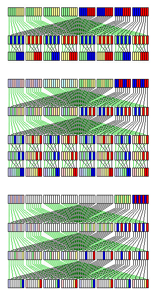
A circuit that simply rearranges the 512 bytes contained in sixty-four data words of 64 bits each from
0 1 2 3 4 5 .... 508 509 510 511
to
0 128 1 129 2 130 .... 126 510 127 511
will, when applied once, move the bytes in consecutive 32-bit operands to consecutive 64-bit data words, thus delivering them to the appropriate ALU, and, if applied twice, will move the bytes in consecutive 16-bit operands to consecutive ALUs with a 64-bit path to cache memory, and if applied three times will deliver consecutive bytes to consecutive ALUs.
But the bytes will not be in the right positions; this can be dealt with by using a circuit with a function that is partially the inverse of this function, but which operates locally on the eight bytes dealt with by each single ALU, that is, rearranging the eight bytes in each of the sixty-four groups of eight bytes from:
0 1 2 3 4 5 6 7
to
0 2 4 6 1 3 5 7
Inverse versions of these two circuits will also be required for returning values to memory.
Given a 64-bit path into each ALU, so that doubleword operands proceed directly from cache into the ALU, the operations shown above for different sizes of operands are:
For word operands, one global scatter operation, followed by one local gather operation.
For halfword operands, two consecutive global scatter operations, followed by two consecutive local gather operations.
For byte operands, three consecutive global scatter operations.
Then, a shift step, if necessary, selects which of the two groups of words, or which of the four groups of halfwords, or which of the eight groups of bytes, in a group of doublewords, is operated on in the bank of ALUs, and finally a masking step removes the unused inputs.
Also, it may be noted that it is not necessary for a long vector operand to be aligned on a boundary representing 64 of the data items of which it consists. The circuitry required to deal with this expeditiously is also useful for more general inter-ALU communications, and is therefore described in a subsequent section concerning a MIMD capability obtained by adding a simple control unit to each ALU.
Note that this type of circuitry appears inconsistent with the use of the Medium floating-point type with long vector instructions. However, the circuitry provided for data memory width control can be used to permit efficient operation on this floating-point type for some combinations of floating-point format and memory width, as follows:
If the memory width provides normal 32-bit words, for most formats the Medium floating-point type may be handled by caching memory containing variables of that type as if it consisted of 24-bit words; for the Standard format, the Medium floating-point type may be handled by caching memory containing variables of that type as if it consisted of 40-bit words.
If the memory width provides 24-bit words, for most formats the Medium floating-point type may be handled by caching memory containing variables of that type as if it consisted of 36-bit words; for the Standard format, the Medium floating-point type may be handled by caching memory containing variables of that type as if it consisted of 60-bit words.
If the memory width provides 40-bit words, for formats other than the Standard format the Medium floating-point type may be handled by caching memory containing variables of that type as if it consisted of 60-bit words.
For all other combinations of memory width and floating-point format, the Medium floating-point type may not be used with long vector instructions.
Note also that values in the Medium floating-point type need to be aligned on 16-bit boundaries, not 48-bit boundaries, and thus caching to deal with these values may involve an offset that would not occur if a memory width of 48 bits is applied to all memory beginning with location zero; however, such offsets can also be used when the memory width is changed normally; the actual restriction imposed on the address associated with a cache line is that it must be a multiple of the width of the data bus to main memory.