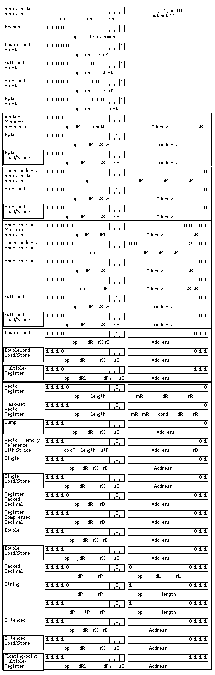
Starting with the following as the basic instruction format:
with 32 fixed-point registers, each 64 bits in length, 32 floating-point registers, each 128 bits in length, and 8 short vector registers, each 256 bits in length. For load and store memory-reference instructions, only integer registers 1 to 7 can be index registers, only integer registers 26 to 31 can be base registers, but all 32 registers may be destination registers. For the standard memory-reference instructions that allow operations, only integer registers 1 to 3 can be index registers, registers 0 to 3 of whatever type can be destination registers, and for floating-point instructions, only integer registers 28 to 31 can be base registers; for fixed-point memory-reference instructions, only integer registers 30 and 31 are allowed instead. (This design choice is due to the fact that having unnormalized floating-point operations from memory for the one floating-point type that supports them, extended precision, has a very low priority, but having Insert and Unsigned Load operations from memory for fixed-point types shorter than 64 bits has a very high priority.)
A jump to subroutine instruction uses the index register field to indicate where the return address is stored; integer registers 24 to 31 are used for this purpose. Thus, a subroutine return would normally be an unindexed jump with a displacement of zero.
The jump instructions have the opcodes:
0000 JSR Jump to Subroutine        1000 JV  Jump if Overflow
0001 JL  Jump if Low
0010 JE  Jump if Equal             1010 JC  Jump if Carry
0011 JLE Jump if Low or Equal      1011 JNC Jump if No Carry
0100 JH  Jump if High
0101 JNE Jump if Not Equal
0110 JHE Jump if High or Equal
0111 JNV Jump if No Overflow       1111 JMP Jump
The clash between conventional conditional-jump instructions of this type and a VLIW architecture is addressed through the uses of the bits that explicitly indicate dependency, to be described below.
For the multiple-register instructions, used for saving registers during subroutine calls, only integer registers 30 and 31 are available as base registers. Their opcodes are:
0 LM    Load Multiple
1 STM   Store Multiple
This format is very cramped for opcode space because all 32 registers can be the source register for a register-to-register instruction; even here, a compromise had to be made, so that only registers 0 to 15 of whatever type could be the destination of a register to register instruction. However, space was found for three-address register to register instructions, where all 32 registers may be the source, the operand, and the destination, and those even have nine bits available to indicate the opcode, which permits extra instructions in addition to the basic set.
The layout of some of these instructions would be:
00 + 7 bits       standard operations on basic types
001100 + 3 bits   register packed decimal operations
001101 + 3 bits   register compressed decimal operations
001110 + 3 bits   RC op RP to RC
001111 + 3 bits   RP op RC to RP
01 + 7 bits       short vector operations on basic types
Note that memory-reference instructions other than byte instructions also cannot have all zeroes in their base register field; this space is reserved. Some of that space, however, is intruded into by the multiple-register instructions.
The intent is that this instruction set, like typical CISC instruction sets, uses only a 16-bit instruction for register to register operations, using a 32-bit instruction only for memory-reference instructions; yet, like a typical RISC instruction set, it has banks of 32 registers available to it, so that it is possible for the compiler to avoid generating code in which consecutive instructions depend on one another.
As with the other example instruction sets I've designed, the instructions correspond to opcode bits as follows:
0000 SW   Swap        1000 I    Insert                 MEU  Multiply Extensibly Unnormalized
0001 C    Compare     1001 UC   Unsigned Compare       DEU  Divide Extensibly Unnormalized
0010 L    Load        1010 UL   Unsigned Load          LU   Load Unnormalized
0011 ST   Store       1011 X    XOR                    STU  Store Unnormalized
0100 A    Add         1100 N    AND                    AU   Add Unnormalized
0101 S    Subtract    1101 O    OR                     SU   Subtract Unnormalized
0110 M    Multiply    1110 ME   Multiply Extensibly    MU   Multiply Unnormalized
0111 D    Divide      1111 DE   Divide Extensibly      DU   Divide Unnormalized
there being eight instructions common to integer and floating point, eight extra ones being used for integer types and a different eight extra ones for floating point types which may be unnormalized.
Multiplication and division are not provided for byte values. The opcode that would indicate a multiply byte instruction, 000 0110, instead indicates the instruction LA, Load Address, which loads a 64-bit integer register with the effective address of the instruction. This is helpful for utilizing those instruction formats which only allow a base register, but not an index register, to be specified. This also applies to the corresponding memory-reference instruction, which begins 1101 0110.
Also, what would be a divide byte instruction, 000 0111, is instead SWBDG, Swap Bytes if Destination Greater, which is required as an atomic operation to facilitate interactions between processes. Again, the corresponding memory-reference instruction begins 1101 0111.
The types are indicated, in seven-bit opcodes, as follows:
000  B   Byte       8-bit fixed point
001  H   Halfword  16-bit fixed point
010      Integer   32-bit fixed point
011  L   Long      64-bit fixed point
1000 F   Floating  32-bit floating point
1001 D   Double    64-bit floating point
101  E   Extended 128-bit floating point
with the letters shown being suffixes to the name of the instruction, and the letter R following as a further suffix to register-to-register instructions.
The shift instructions are:
000 SHL  Shift Left
001 SHR  Shift Right

011 ASR  Arithmetic Shift Right
100 ROL  Rotate Left
101 ROR  Rotate Right
110 RLC  Rotate Left through Carry
111 RRC  Rotate Right through Carry
In the case of three-address register-to-register instructions, the registers specified as the destination register and the operand register may be the same, and then the instruction will behave as a two-address register-to-register instruction.
One thing that may be noted from the diagram is that the sizes of fields in which registers may be specified vary considerably from one type of instruction to another. This is a consequence of dealing with a very constrained opcode space.
One thing that constrains the opcode space is that, following my practice with other ISAs that I have constructed, I provide displacement fields that permit a region of 65,536 bytes to be addressed starting from the address value in a single base register, and I permit indexing with that as well, in a memory-reference instruction that occupies no more than 32 bits.
In comparison, the IBM 360 allowed base/index addressing in 32 bits, but limited the displacement field to a 12-bit one that could only reach 4,096 bytes. The Motorola 68020 allowed a base register and an index register to be specified, with a 16-bit displacement, but only if the instruction was 48 bits long.
So, in my original proposed architecture, I began with the compromise of having sets of eight registers instead of sixteen; then, as I sought to include more capabilities in shorter instructions, I went on to use the idea of only allowing aligned operands to be referenced in order to make additional opcode bits available, which I became aware of from the SEL 32 computer.
This continues here, even though I have moved bits from the opcode to the destination register field as I have emphasized load/store instructions of the RISC type, and provided banks of 32 registers.
This short table shows the different ranges of registers from within the 32 available in the three main register banks (only the roles of source and destination register, however, also apply to the floating-point registers and the vector registers) that can be used for different purposes:
Destination Register
  0 to 31:
   Three-address Register to Register
   Vector Register
  0 to 15:
   16-bit Register to Register
  0 to 7:
   Vector Load/Store
   Mask-set Vector Register
  0 to 3:
   Byte, Halfword, Fullword, Doubleword, Single, Double, Extended CISC Memory Reference
  0 to 1:
   16-bit Shift

Source Register
  0 to 31:
   Three-address Register to Register
   16-bit Register to Register
   Vector Register
  0 to 7:
   Mask-set Vector Register

Index Register
  1 to 7:
   Byte, Halfword, Fullword, Doubleword, Single, Double, Extended Load/Store
   Short Vector Load/Store
   Jump
  1 to 3:
   Byte, Halfword, Fullword, Doubleword, Single, Double, Extended CISC Memory Reference
   Short Vector CISC Memory Reference

Base Register
 24 to 31:
   Vector Load/Store
 26 to 31:
   Byte, Halfword, Fullword, Doubleword, Single, Double, Extended Load/Store
   Jump
 27 to 31:
   Short Vector Load/Store
 28 to 31:
   Single, Double, Extended CISC Memory Reference
 30 to 31:
   Byte, Halfword, Fullword, Doubleword CISC Memory Reference
   Short Vector CISC Memory Reference
   Doubleword, Extended, Short Vector Multiple Register

Mask Register
 0 to 31:
   Vector Register
 0 to 7:
   Mask-set Vector Register
Unlike the fixed-point and floating-point registers, there are only eight short vector registers, and the three types of short vector register instructions can access all of them.
There are 32 vector registers, each of which may contain space for 32 64-bit floating-point numbers. It is possible an extension to the architecture, involving 48-bit or 80-bit and 96-bit instructions, as described below, may also allow vector operations on other data types, including 128-bit extended precision floating-point numbers.
The short vector operations are similar to the vector extensions provided with many popular microprocessors today, while the vector operations are instead modeled after the capabilities of vector supercomputers such as the Cray I and its successors, so the two should not be confused.
Instead of simply being placed in memory one following another, these instructions may be organized into 256-bit blocks by a scheme which can produce results like the example illustrated below:
D1 D2 01 02 03 04 05 06 07 08 09 10 11 12 13 14
D1 D2 15 16 17 04 18 19 20 21 22 23 11 24 25 26
Each item in the diagram above is 16 bits long. D1 and D2 represent a 32-bit header for the block which indicates which instructions depend on each other. The numbers indicate the instructions themselves, in the order of their execution.
When an instruction is 32 bits long, its two 16-bit halves, instead of directly following each other, are in consecutive blocks in matching positions. This is shown for instruction 04 and instruction 11 in the diagram above. So the top line contains the numbers from 01 to 14 in order, but a second 04 and a second 11 drops down into the next line, and the instructions from 15 to 26 must skip around them.
To avoid possible confusion, it will be emphasized that: this skipping is a direct and automatic consequence of instructions 04 and 11 having been found to be 32 bits long in the decoding of the previous block, and does not require a branch of any kind in instructions 17 and 24 to effect it; rather, the decoders for the positions occupied by instructions 04 and 11, being busy with the decoding of instructions associated with the preceding block, will not decode and issue instructions associated with the block containing instructions 15 through 26.
Thus, in general, because a block will tend to contain some 32-bit instructions, the block following a given block will have to be read before the instructions in that block can be executed.
It is unclear, though, I must admit, whether this scheme has a real benefit. Since it is simple to determine if an instruction is 16 or 32 bits long by its first few bits, all that is saved, at the cost of having a constant delay by being required to read the next instruction block, would be a few gate delays at the beginning of instruction decoding.
But even a few gate delays in every cycle is an impediment to speed, while a delay is only endured once - or, at least, once when a program starts, and once for every branch that takes place.
The 32-bit dependency header at the start of each block has the following format:
Offset: 4 bits
Instruction depended upon: 14 bits
Dependent instruction: 14 bits
Normally, the offset field will contain a number from 0 to 14. That indicates how many 1 bits one has to skip in the "Dependent instruction" field in order to find the 1 bit, corresponding to the start of an instruction that depends on something, which corresponds to the instruction which depends on the instruction the start of which is indicated by the first 1 bit in the "Instruction depended upon" field.
Note that the offset value can be such that one would have to continue skipping 1 bits into the next block, or even a later block than that.
Thus, the offset will lead to correspondences between instructions like this:
Dependency field:
0101 10100110101101 01101101100110
     a b  cd e fg h  ** ** *a  bc
As there is a 5 in the offset field, the five asterisks indicate the five one bits to be skipped over in the dependent instruction field as indicating dependency on something in the previous block rather than the current block.
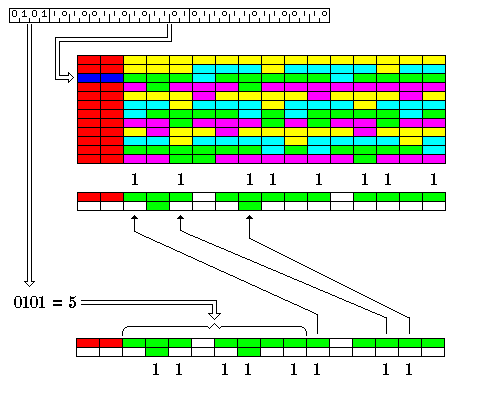
The diagram above illustrates not only how the dependency bits work, but also the general instruction format. The 32 bits of dependency information are shown for the third of twelve blocks; this is indicated by showing the dependency bits of that block in blue, and those of other blocks in red.
The instructions belonging to each block are in different colors, alternating between yellow, cyan, green, and purple in sequence three times. This shows how, when a 32-bit instruction comes along, its second half is in the corresponding position in the next block.
Then the instructions for that third block are illustrated, twice, at the bottom, once associated with the bits indicating instruction on which there is a dependency, and once associated with the bits indicating an instruction is dependent. Since it's the 1 bits that are significant, only they are shown, and it is also shown how the offset indicates the number of 1 bits in the dependent instructions part to be skipped within a given block to keep the two sequences of bits, the ones indicating the instructions depended upon, and the ones indicating the dependent instructions, synchronized.
If the offset field contains 1111, then there may be two additional 16-bit units of supplementary information present in the block, if instructions longer than 32 bits are provided for. (It is necessary for the 16-bit units corresponding to them in the preceding block not to be the first unit of a 32-bit instruction in that case.)
The first four bits of the first of these units contains the offset, which is still needed information. The remaining twelve bits of that unit contain a 1 bit corresponding to every unit of the remaining twelve units in the block that is the first unit of an instruction, whether 16 or 32 bits in length.
The second unit contains bits which should normally all be zero, but which are reserved for use to cope with a provision, to be described below, to permit instructions longer than 32 bits to be handled by this architecture.
Initially, I thought that the number of bits available was too short, by one, to allow only three units of prefix information to be used, but I had forgotten something.
Instead, as it appears that instructions longer than 32 bits in length can be avoided entirely, while the third unit of 16 bits would have the format described above, the extra thirteenth bit required to indicate if the first unit of instructions following is, or is not, the beginning of a new instruction would replace the first bit of the 14 bits used to indicate dependent instructions - since now there is one bit available in each field.
This format is illustrated below:
Thus, the zero bits in that field, entirely (in the case of a four-unit prefix) or mostly (in the case of a three-unit prefix) in the third unit of the block, indicate what to skip in the event that an external branch into the block takes place.
There is one case in which the contents of the dependency field affects what an instruction does instead of merely ensuring the instruction can execute correctly in the absence of interlocks to detect dependency.
A conditional jump instruction either jumps or not depending on the condition codes left at the completion of the instruction on which it is marked as dependent rather than those left by the immediately preceding instruction. This scheme permits the same instruction set to be used conventionally or within the VLIW structure outlined here, as opposed to a branch followed by delay slots, or the use of flag bits, which require changes to the instruction set; instead, the burden of coping with the special efficiency requirements of VLIW is placed in the annotations to the instruction set.
There is a limit on this facility: only the condition codes of the 32 most recent instructions are retained.
Also note that no mechanism is specified for indicating that two instructions in the same instruction block, although not dependent, cannot be issued on the same cycle, but must be issued on consecutive cycles, due to a conflict in the use of available ALU faciliies. This is for two reasons:
The first instruction block of a program module does not need to have one (or two) extra 16-bit units of prefix information. Thus, if a branch takes place into an instruction block that does not have the prefix bits equal to 1111, it will be assumed that that block begins a routine, and that all fourteen positions in the block that may contain the start of a new instruction in fact do so. Given this, the prefix bits for such a block should normally be 0000, and this could be used as a sanity check for branches. As well, a branch should not be to one of the units containing prefix information; however, branching to the very beginning of an instruction block may be used in the future for a special purpose.
Note that even instructions providing vector capabilities similar to those of the Cray I have been made to fit within a 32-bit length limitation, in unused portions of the opcode space.
There are 32 vector registers, each containing 32 elements. Only vector operations on 64-bit floating-point numbers are provided, not on any other data type.
Only load or store operations are provided between vector registers and memory. The primary instruction format for those does not include stride; another one is present that allows one of integer registers 16 through 19 to be specified as containing the stride; this one is limited to vector registers 0 or 1 as the destination, and integer registers 30 or 31 as the base register.
For operations between vector registers, the eight basic floating-point operations are provided. Integer registers 1 through 31 may be used as mask registers; if 0 is indicated in the mask register field, masking is not requested.
An alternate form of the vector register instruction is provided, where a condition is specified using the same coding as used to specify a conditional jump instruction. In this way, the least significant 32 bits of an integer register may be set according to whether the results of a vector register operation meet the given condition, so that this value may be used later as a mask for another vector register instruction.
The length field is always a full five bits long, so that vectors of arbitrary length can be handled using multiple vector instructions, the last of which handles the elements in excess of an exact multiple of 32.
Also provided are Short Vector instructions, which are similar to the families of instructions known as SSE or AltiVec on many current popular microprocessors. The Short Vector instructions work on 256-bit long operands that may be subdivided into bytes, halfwords, integer or long integer items, or single-precision, double-precision, or extended-precision floating point items. Thus, since all the basic operations on the basic types are applicable to them, they were given seven-bit opcodes.
Originally, the fixed-point registers were used, four at a time, to contain a short vector; however, as this would lead to a conflict with the use of some of those registers as base registers, once it was clear that it would be possible to find opcode space for short vector multiple register instructions, a convenience for context switching, that particular compromise was abandoned.
While I have attempted to make this architectural description fairly complete, it doesn't include things like privileged instructions, such as the return from an interrupt, or the format of the program status word. Also, one thing that is omitted, but which would seem to be highly desirable for a high-efficiency architecture, is some type of loop instruction that repeats a sequence of instructions a fixed number of times, thus avoiding the overheads of conditional branching when they are not needed.
Note that among the memory-reference instructions squeezed in at odd portions of the opcode space are instructions for register packed decimal and register compressed decimal. Both types are 64 bits long in memory. Register compressed decimal operands are 19 decimal digits long, consisting of one packed decimal digit followed by three 10 bit fields in Chen-Ho encoding containing three decimal digits.
Register packed decimal quantities are placed in the integer registers, which are 64 bits wide. Register compressed decimal quantities are expanded to packed decimal, and then placed in the least significant bits of a 128 bit wide floating-point register, with other bits set so that the value can be left undisturbed by extended-precision load and store instructions.
Otherwise, an additional multiple-register load and store instruction pair, presumably for an additional set of 32 registers, each 76 bits wide, would be required.
In both cases, numbers beginning with 0 to 9 are positive, and numbers beginning with A through F are taken as negative numbers in ten's complement form.
Also, since there is a Load Address instruction, it is possible to squeeze into a 32 bit format instructions similar to the 48-bit packed decimal and string instructions of the System/360. Since many RISC machines use one instruction to add an index register to an address, and another to perform the actal memory-reference instruction, it was felt this was not so wasteful as to be unusable.
It is intended that the machine be capable of executing programs both with the VLIW organization described here, and also in conventional CISC form, where the 16 and 32 bit instructions just follow one after the other, with conditional jumps depending on the results of the immediately preceding instruction.
One likely configuration would allow only one thread to contain a program in VLIW mode; there would be multithreading, providing for either sixteen concurrent threads in conventional CISC mode, or one VLIW thread and two CISC threads. Or it might be desirable to double those numbers, allowing either two VLIW threads plus four CISC threads, or thirty-two CISC threads - or one VLIW thread and eighteen CISC threads.
Multithreading potentially does a better job of keeping all the functional units of a processor fully utilized than even a carefully crafted VLIW program is likely to be able to. However, VLIW still as the advantage of making a single thread able to use as much of the processor as possible, thus reducing the latency of that particular thread.
Incidentally, though, if savings are realized by the VLIW format, which explicitly indicates dependencies, that would mean that circuitry for detecting dependencies to provide interlocks would be omitted. Certainly, as such circuitry is complex, it would require more gates than such things as a buffer for thirty-two sets of condition codes. So not only would it not provide out-of-order execution of CISC code, consecutive instructions would not have their execution portions overlapped, with only different threads being treated as independent.
This implies the possibility of error if something in one thread does depend on something in another thread (despite using different sets of registers, they could refer to the same location in memory) in addition to the significant limitation on performance.
Given, however, that interlocks to detect dependencies are a very standard featre of pipelined computers, RISC or CISC, this may not be the actual situation. Instead, in the case of a 32-thread system, what might happen is that the system would have the capacity to support two VLIW threads and four fully-interlocked CISC threads, but then the additional CISC threads which become available when the number of VLIW threads is less than two, that is, when there are no VLIW threads, or there is only one VLIW thread, are not interlocked, and are thus subordinate, as they can only use, at most, a smaller share of system resources than the faster-running fully-interlocked CISC threads are capable of using.
If code in VLIW format and CISC format can coexist in the architecture, rather than making switching a privileged operation, it makes sense to allow code of both types to call library routines supplied in only one format.
The simplest way to modify the architecture to provide for this is to limit virtual addresses to 62 bits. This should not be a bad thing, given that it is unlikely for a full 64-bit address space to ever be used, despite the precedent of the System/360 having to increase, first from 24 bits to 31 bits, then to a full 32 bits, and then beyond 32 bits to 64 bits, since all the microprocessors today that have a 64 bit mode actually only use 48 or fewer bits of the address on their address bus.
When the first bit in a 64-bit address is a 1, that indicates that the second bit in that address specifies the mode to use: 0 meaning CISC mode and 1 meaning VLIW mode. When a JSR instruction uses such an address, the return address will also contain an address with the first bit set, so that the mode will be restored upon return.
In creating this architecture, I started out with the basic idea of the new VLIW-style instruction arrangement that still allowed variable length instructions. The motivation was that in many quarters, variable-length instructions are regarded as highly inefficient; yet, allowing instructions to vary in length increases the efficiency of instruction encoding. Other attempts, such as "Heads-and-Tails encoding" have been made to address this.
As noted above, since whether an instruction is 16 or 32 bits long is very simply indicated by its first few bits, one is trading off a very limited number of gate delays in instruction decoding for a delay of the loading of one instruction block before execution can begin. But this delay is a "one-time" loss of time - once when a program starts, and also once every time there is a branch.
Thus, it will be legitimate to question whether this elaborate feature is present for a rational purpose, or is just there for marketing reasons. To permit that question to be answered by direct benchmarking by the customer, perhaps a mode where there are still 32 prefix bits in a 256-bit instruction block, indicating dependency, but the variable length instructions simply follow one another in order as in CISC mode, should be provided.
This would continue to have the other features of VLIW mode; for example, condition codes would be buffered, and the dependency bits would control which set of condition codes applies to a conditional jump instruction. (Thus, one thread of this new mode would still be equivalent to fourteen CISC threads.)
That would add to the complexity of the instruction decoding system; if the extra gate delays can be switched out of the system for true VLIW mode, and this results in an actual saving of a cycle somewhere, even though those few gate delays don't take a whole cycle themselves, that means that instruction decoding would have two sets of Earle latches in it so as to be broken into stages in two different ways.
In itself, though, a DSP-style VLIW arrangement is only useful if there is a lot of instruction-level parallelism. Register-to-register instructions tend to be only 16 bits long in CISC architectures... with up to 16 registers. But to have instructions interleaved which don't depend on one another, so that while one instruction is executing, other unrelated instructions can be started, before the next instruction that require its result starts, one would like to have more registers. At least 32 registers, as is used with many RISC systems.
And I managed, barely, to squeeze in 32 registers - by restricting the destination register to be one of the first 16.
The idea used in the SEL 32, of having essentially the same instruction act on operands of different types, by allowing only aligned operands, and putting a distinctive code in the unused bits of the address, allowed the 32-bit memory-reference instructions to be squeezed in what remained of the opcode space. This also required some rather less-than-orthogonal use of the set of 32 registers; only the last seven could be base registers, only the first four could be the destinations of a memory-reference instruction, and different, usually more severe, restrictions applied to the other odd instructions squeezed in to odd spaces left between the initial common types of memory-reference instructions.
The diagram of the instruction formats is now organized to make the instruction decoding more understandable; the 32-bit instructions are divided into boxes, one for each of the possibilities for the last few bits of the address under this scheme (there are also three major divisions, byte instructions, other fixed-point instructions, and floating-point instructions, not specifically indicated by a heavier border - the jump instructions belong with the floating-point instructions), and within those boxes, the memory-reference instructions for the primary data type those bits indicate now have their label enclosed in a box to emphasize it, with the other types of instruction squeezed into leftover opcode space not used by the primary data type are not so emphasized.
Thus, for example, when an instruction begins with 1111, and the final bits are 01, the primary data type is single-precision floating-point. Vector Memory Reference with Stride Load/Store instructions are squeezed in using the most common technique, using the opcode space yielded up by placing 000 in the base register field of what would otherwise be a single-precision floating-point instruction. The Register Packed Decimal and Register Compressed Decimal memory-reference instructions, on the other hand, are squeezed in by setting the first opcode bit equal to 1 instead of 0; this is possible because single-precision floating-point is floating-point type with a hidden first bit; therefore, the unnormalized instructions are not required, and that opcode bit is available to expand the instruction set.
Instructions longer than 32 bits can potentially be handled in this design, but with some serious restrictions.
The shift instructions with the unused opcode 010 can be used as prefixes to modify the corresponding instruction that begins in the next block. In this way, the beginning of the last 32 bits of the instruction indicates the position of that instruction in execution order.
Because the block containing the required prefix bits would not have been read, branching into a block that contains the second 16 bits of a 48-bit instruction at a point prior to that unit would result in an incorrect result; they would be read and executed as the 32-bit instruction they would be in the absence of a prefix. The last 16 bits, on the other hand, can just be skipped like the last 16 bits of a normal 32-bit instruction.
In the case where the second 16 bits of a 48-bit instruction would be read as a 16-bit instruction instead of a 32-bit instruction, then it would appear that they could not be present in any position in a block that is a branch target, as a loss of synchronization would result. However, this problem may be addressed through the use of the 16 bits in the header portion of a block containing a branch target that were noted as unused and reserved above.
The intent is to insure that the maximum delay imposed by the instruction format befor a 16-bit instruction can execute is the wait for the following block to be read, containing the final parts of the 32-bit instructions in the same block. So the instruction format with some 48-bit instructions becomes:
D1 D2 01 02 03 04 05 06 07 08 09 22 10 11 12 13
D1 D2 14 15 16 17 05 18 19 20 21 22 23 11 24 25
D1 D2 26 27 16 28 29 30 19 31 32 22 33 34 24 35
the 32-bit instructions continue from one block to the following one, but the 48-bit instruction is anticipated by its first 16 bits, its second 16 bits occupy its nominal place, and its last 16 bits are in the block following.
This allows including things like string instructions and more elaborate vector instructions (i.e. vector operations with the stride value in the instruction, vector operations on types other than double-precision float) to the architecture. While instructions like the memory-to-memory packed decimal and string instructions of the IBM 360 would not seem to accord with the goal of high efficiency, although better implementations that do not involve repeated single-byte accesses to memory are possible, vector instructions like those of the Cray I clearly are another way to efficiently exploit parallelism.
As a prefix code sets a flag in the instruction decoder that read it, and leaves supplementary information for executing the instruction that follows, theoretically the length of the following instruction could be allowed to be 16 bits instead of 32 bits, perhaps by having its length be decoded according to the normal rules.
This would be confusing, however, in that now there are two kinds of 32-bit instructions, "real" 32-bit instructions whose place in execution is determined by their first 16 bits, and prefixed 16-bit instructions whose place in execution is determined by their last 16 bits.
This VLIW format avoids the need to read the 16-bit units of instructions one at a time, since if there is a 32-bit instruction, the next 16 bits are in the next block. Since prefixes provide advance warning to the instruction decoder to shift gears, though, a pair of suitable prefixes switching to a 32-bit decoder so as to allow a 96-bit instruction - two 16-bit prefixes in the block preceding the long instruction's place, the 32-bit middle part of the instruction in the next block, and the 32-bit conclusion of the instruction in the final block would not be insuperably complex, and would avoid having instructions that span more than three blocks, even if longer instructions are required.
A switch to a 32-bit decoder suggests that these kinds of extra-long instructions might have to be aligned on 32-bit boundaries in the blocks.
One possibility would be to allow both 80-bit or 96-bit instructions; a prefix could occupy either or both of the 16-bit units preceding the 32-bit aligned pair of 16-bit units to be affected; thus, there would be three series of extra-long instructions, types 80A, 80B, and 96.
In the case of an instruction block that is a potential branch target, instructions that span three instruction blocks, whether they are 48 bits long or 80 or 96 bits long, are handled as follows:
The least significant 12 bits of the fourth 16-bit unit of the prefix field are used for the special indications required.
Incidentally, one way to allow the prefix area of a block that is a branch target to usually only consume 48 bits instead of 64 bits, and yet allow 80 and 96 bit instructions, would be to have the offset value of 1110 indicate the four-unit prefix required when a branch target also intersects these longer instructions. That would be useful because it is expected that even if the longer instructions are provided, they will be extremely rare in practice. Also, limiting offsets to the range 0 through 13 instead of 0 through 14 should not be a serious issue.
Before deciding that it is necessary to more generally fulfill the promise of the design to offer everything that a RISC design does, by allowing load/store instructions that have all 32 registers as their destinations, I thought of a different alternate mode which would perhaps allow early fetches of operands.
Since only the first 16 registers could be destinations for the 16-bit register-to-register instructions, I thought it would be adequate, in an alternate mode, to take the four instructions for the four basic arithmetic operations, add, subtract, multiply, and divide, and instead make them into a single instruction, Operation Prepare, taking two opcode bits, and joining them to the destination register field, to allow 16 possible destinations.
But the destinations would be 16 "shadow registers", associated with the first 16 registers in each register bank. The actual operation, which would take place later, whether add (or any other of those four) or XOR (or any other not of those four), would be performed by register-to-register operations that named the same register as the source and the destination.
The idea there was to avoid increasing the opcode space needed. But the extra machine state in the shadow registers would complicate things like interrupt handling, although things like saving the last 32 condition codes already create that problem for VLIW operation.
An alternative to this which would accomplish the same thing, but perhaps be easier to understand, would be to have instructions that read data from memory, but which, instead of putting it in a register, or in a shadow register associated with a register, or in a dataflow node construct of some kind, put the data from memory on a queue internal to the CPU. Then, later instructions could pop the data from the other end of that queue and perform a desired operation with it.
To avoid confusion, it should be noted that because the data may arrive outside of the required order, this can't actually be implemented as a stack. The actual data would have to be in conventional addressable storage, which would look like a stack when data is read out, by being implemented as a circular buffer. The addresses would be given to circuitry which would immediately request the data in question from memory; and the tag with which the data item would be recognized when it arrives would have to be placed in a content-addressable memory, so that upon arrival it would be possible to retrieve where to put the actual data.
However, these are very standard implementation techniques, which I had thought unworthy of mention.
This makes more sense if fetches from memory complete in a strictly sequential fashion. However, sometimes data sought from main memory is already in the L2 cache, and sometimes it isn't.
If one could claim that this mechanism, by permitting requests for data to be scheduled far enough in advance, was so wonderful that we didn't even need a cache because of it, that would be one thing. But, of course, that's too ridiculous to have any chance of being true. Since, however, while a cache would continue to make a great contribution to performance, those items of data which are being requested so far in advance by this proposed technique really wouldn't benefit much by being in a cache, this suggests that a compiler should only use the technique for data which, at least, has a real chance of not being in the cache (although mistakenly not using the technique when it can help has worse consequences than using it when it's not needed).
If this technique were to be used, the same method could be used as with Shadow Register Mode to indicate when the operation is to be performed: a two-address register-to-register instruction with the same source and destination register could indicate that the source operand is instead taken from the stack.
The fetch instruction could be indicated by removing register 3 as a possible destination register for the (memory-reference) Swap instruction; that which would be a Swap instruction with destination register 3 would instead be a Fetch instruction, that initiates a fetch from memory, with the result to be placed on the operand stack.
One way to use this would be to unroll the first iteration of a loop, use the Fetch instruction for that first iteration, because the operands are unlikely to be in the cache, and use the ordinary CISC-style memory-reference instructions for the later iterations, where the data is now likely to have been prefetched to the cache.
One of the rationales behind the design of VLIW signal processing chips is to permit high performance while saving costs. Thus, the cost of putting in pipeline interlocks is saved by including bits that explicitly indicate instruction dependencies.
An even larger cost that RISC designs are often aimed at saving is the cost of implementing out-of-order execution.
A computer with an out-of-order pipeline can improve single-thread performance by executing instructions from later in the instruction stream while it is waiting for a dependency to be resolved. To do this, it uses extra hidden registers which allow such later instructions to be executed, even if they are re-using the same register as some of the older instructions that are waiting to finish.
A RISC architecture reduces the need for out-of-order execution in two ways.
Retrieving data from memory takes a long time, compared to internal computations, on today's microprocessors. A normal memory-reference instruction that, for example, adds a number found in memory to the contents of a register, can't be started until that register's contents are already present.
On a RISC machine, though, one would simply first load another register with that value from memory, and that doesn't depend on the value to which it will be added. The register-to-register add instruction can come much later in the program.
On a pipelined machine, most instructions take several cycles to execute, but it is desirable to have the machine start a new instruction every cycle.
So instead of putting the next dependent instruction in a desired sequence of operations immediately after its predecessor, the instructions to carry out other calculations should be interleaved with such a sequence, to keep the computer busy.
On a RISC machine, instead of having eight or sixteen general registers, there may be thirty-two or more such registers, which makes it more practical for the computer to be doing unrelated things'' concurrently.
However, despite this, most of today's RISC microprocessors are out-of-order designs, despite this adding considerable cost and complexity to a microprocessor. Why?
Most currently popular RISC microprocessors have sets of 32 general registers. This is enough to allow a limited number of computational sequences to be interleaved in the manner described in the second point above.
This is adequate if instructions take a limited number of cycles to execute. However, as designers have sought to produce higher performance designs, they have increased the number of pipeline stages. This means that a larger number of computational sequences need to be interleaved in order to fill the cycles between successive instructions belonging to the same sequence.
And that means that 32 registers may no longer be enough.
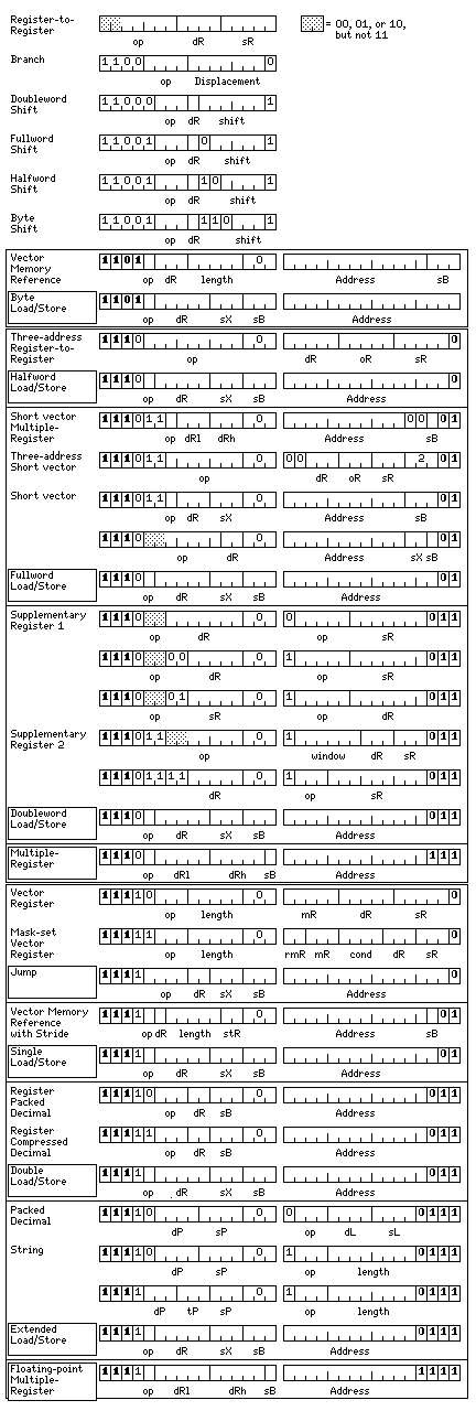
And so in the one remaining area of unused opcode space, I've added Supplementary Register 1 instructions, which are register-to-register instructions that work on a set of 128 registers, and Supplementary Register 2 instructions, which work on a set of 512 registers.
In the case of Supplementary Register 1 instructions, there are register-to-register instrctions that work between any two of them, or between one of them and the 32 original registers.
In the case of Supplementary Register 2 instructions, the register-to-register instructions work between two registers in the same group of eight register, and there are also load-store instructions between that set of registers and the 32 original registers. Note that three bits are required to specify a load-store operation, because a fixed or floating load at any precision can be specified.
An additional change to cope with a deeper pipeline would be to double the length of an instruction block, and of the dependency field in the front of the block. In this way, the offset field becomes eight bits long, and that will allow detailed dependency information to be given for more deeply interleaved code.
Also required is some way to allow the multiple independent sequences that are interleaved to be separated, so that any or all of them can loop independently of the others, or even carry out conditional branches. Since a portion of the same basic register banks would be used, rather than a separate set of register banks, this would not be the same as multiple threading, but it would still involve multiple program counters and multiple sets of condition code bits.
Useful additional instructions for this situation will be coded as follows:
As a jump instruction with opcode 110 (subsuming 1100 and 1101), XL (Execute Loop). The shorter opcode expands the dR field to three bits from two. The dR field is used to indicate the count register - the register containing the number of times to execute the loop. The dX field is used to indicate the length register - the register containing the number of instructions in the loop. The dB field is used normally, indicating the base register to be used with the displacement.
Once the final iteration of the loop is performed, control returns to the instruction following the XL instruction.
As a jump instruction with opcode 1110, SBS (Start Basic Subthread). This initiates the execution of a basic subthread at the destination address. The instructions in a basic subthread simply follow one after the other as in a normal CISC processor, and the next instruction does not execute until the preceding one completes (all instructions are assumed to be dependent on the one preceding). A maximum of 128 basic subthreads, in addition to the main subthread of a given thread, may be active at any one time.
The dR field is interpreted as follows:
Note that this permits a basic subthread to perform register packed decimal and register compressed decimal operations with the supplementary registers in its own register window, instead of being constrained to perform all such operations using the primary 32 registers.
A subthread may initiate another subthread; and it is not constrained to impose the same register window on subthreads it creates as may be imposed on it. Thus, such subthreads are not to be regarded as nested.
The current register window in effect does apply to loops initiated by the XL instruction.
Also required is a subthread terminate instruction, to remove a subthread from the list of those for which fetch and execute will be attempted. This opcode will be defined within the range of three-address register-to-register instructions, when I also define, within that range and near the end of it, single-register instructions.
The intent is to permit a program to interleave multiple calculations, using different subsets of the available registers, even when some of those calculations will include loops and other control structures, making them no longer amenable to being interleaved directly in the main code sequence.
Also, given that this design is oriented to high efficiency, and to eliminating the need for out of order execution, the ordinary memory-reference instructions have been removed, leaving only the load-store memory-reference instructions. This makes an extra base register available for them.
Recently, a talk was given by John Gustafson, who has impressive credentials as the winner of the first Gordon Bell Prize, as the former director of Intel Labs, and as a former Senior Fellow and Chief Product Architect at AMD, concerning a proposal for a new floating point format called UNUM.
One of the characteristics of this format was that the lengths of floating-point numbers would be dynamically variable, in bits, somewhat like the way that the lengths of strings in many old BASIC interpreters were dynamically variable in bytes.
As the purpose of this was to save on the overhead of data transfers between the CPU and memory, it seemed like a very strange idea to me, as it would actually increase the amount of data transferred between the CPU and memory, as long as conventional memory was used.
Thus, that part of the idea seemed to be something far-fetched, as before DRAM parts were made that embodied such a format, its advantages would have to be seen as compelling, so that they would be widely accepted.
However, I have advocated allowing more flexibility, in a conventional static manner, in the lengths of floating-point numbers.
Other ideas he presented as part of the description of the format seemed reasonable to me.
One was to include an inexact bit in the floating-point format. I agree that this makes more sense than treating an inexact condition as a trap (an interrupt caused by an arithmetic failure in the program, such as an overflow or division by zero), since a trap involves a large overhead, but more especially because an inexact result may not be a failure, but instead is merely something one would desire to keep track of during a calculation.
Another was to specify directly the number of bits in a floating-point number used for the exponent and for the significand (mantissa) individually. Due to the overhead this involves, I think that I will avoid that.
Another was to use the length of the significand as a way of keeping track of the effective accuracy of a floating-point number. As this is in units of whole bits, if one gives up on the idea of making the length of the number dynamically variable, this is equivalent to an old form of significance arithmetic, where numbers are kept in an unnormalized form if their precision is less than that made available by the length of the mantissa field.
Using the idea I had on this page to allow floating-point formats of unusual widths to be handled efficiently, the following set of floating-point formats could be made available:
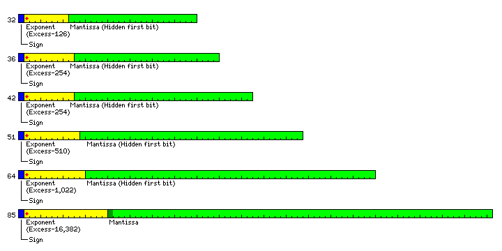
In addition to the conventional 32-bit single precision, 64-bit double precision, and 128-bit extended precision (not shown in the diagram, but having the same structure, except for a longer significand, as the 85-bit format which is shown there), if a 256-bit data bus to memory is used, the following additional widths become available:
In addition, there would be an option for all the formats to avoid the use of a hidden first bit, so as to allow them to be unnormalized to keep track of precision (although this would not apply to the 85-bit and 128-bit extended formats, which already do not have a hidden first bit) and to also replace the least significant bit of the significand with an inexact bit (0=exact, 1=inexact).
If this architecture were to support these additional floating-point formats, however, additional opcode space would have to be made available.
The thought of supporting at least some of the ideas connected with the UNUM floating-point format led me to the realization that more opcode space would be needed.
While a way of supporting 48-bit and 80 or 96-bit instruction formats was outlined above in connection with the instruction block format intended to make variable-length instructions as easy to handle as fixed-length instructions described above, that scheme struck me as awkward (it arose from the desire not to have to fetch ahead more than one 256-bit instruction block).
Even leaving out a need for more instructions to support different floating-point formats, this block format was resource-intensive as the intent was to have a block be fed into fourteen instruction decoders working in parallel.
The discussion concerning adding registers to the architecture in order to permit an efficient in-order implementation even when the number of pipeline stages in an implementation is increased, therefore, led to the subthreads consisting of variable-length instructions that simply followed each other one after another, in the conventional manner; this would entail a return to sequential decoding, although, as the subthreads would consist of instructions to be executed serially with many cycles between them, that would not be a serious issue.
In any event, the diagram below illustrates an alternative method of handling variable-length instructions while allowing rapid decoding.
The portion of the diagram at the lower left shows the scheme to be proposed, and it may strike some people as immediately familiar. There is an old saying, "If you're going to steal (ideas), steal from the best". And thus, my inspiration is the Control Data 6600 computer, designed by the great Seymour Cray. (The 6600 had a 60-bit word, and thus instructions were made from 15-bit pieces, not 16-bit pieces; as well, this scheme is not identical, only similar, to that of the 6600.)
First, though, look at the top right corner. This shows one possible way of quickly decoding instructions that can be either 16 or 32 bits long, with the two parts of the instruction coming one after another, rather than being in successive blocks.
Read 32 bits at a time; if it's a 32 bit instruction, take it; if it begins with a 16-bit instruction, take the 16-bit instruction, and ignore the rest of the 32 bits.
This allows complete flexibility in mixing 32-bit and 16-bit instructions, but it wastes space.
So the next diagram, a little ways to the right, shows an alternative: if the 32 bits begins with a 16-bit instruction, then the other half of the 32-bit block must be a 16-bit instruction.
Green is used to indicate instructions with opcodes characteristic of 32-bit instructions, and yellow is used to indicate instructions with opcodes characteristic of 16-bit instructions.
Thus, the second 16-bit instruction in a 32-bit block is shown as a yellow block with a green line on the bottom; this indicates that if an instruction in that position starts with bits indicating a 32-bit instruction, instead of taking that as an error, one could add in that portion of the opcode space additional 16-bit instructions that can only occur in the second 16 bits of a 32-bit block.
On the lower right of the diagram is a legend showing the classes into which instructions might fall.
Yellow stands for 16-bit instructions. Green stands for 32-bit instructions. Blue stands for 48-bit instructions. Red stands for 64-bit instructions.
The packed decimal instructions and most string instructions might have their opcodes placed in the blue class, since the 32-bit form provided above is limiting, requiring the two memory addresses they use to be placed in pointer registers beforehand. The string instructions such as translate which have a source address, a destination address, and a translate table address, would go in the red class. As it turned out, though, actually all the string instructions, as well as the packed decimal instructions, needed to go into the red class and not the blue class.
Another class is shown as indicated by a dark blue-green color.
These instructions usually have a 32-bit form, and only go to their longer 48=bit form if they begin in the second 16 bits of a 64-bit block, not if they begin in the first 16 bits, even though the space is available.
The floating-point load/store instructions are envisaged as having their opcodes placed in that class, so as to permit a 48-bit form that can handle the new sizes of floating-point operands that might be added, while not significantly reducing the availability of the normal 32-bit form of those instructions.
This would make available additional instructions such as the following:
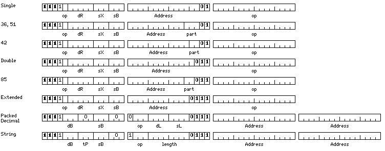
For the string instructions, in the 64-bit form, the translate table still has to be indicated by a pointer; I had originally hoped to use just 48 bits for the string and packed decimal instructions where a translate table is not specified, but there was not enough unused space in the instruction format.
Perhaps a larger version of the diagram might make things clearer:
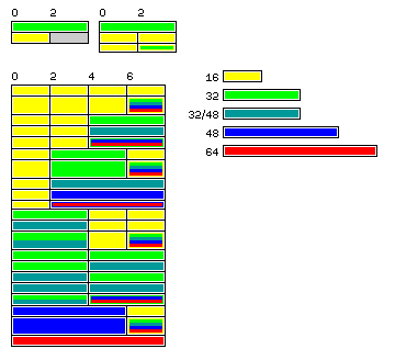
The various combinations depicted as fitting into a 64-bit block are:
  -----------------------------------------------------------
 | 16 bit       | 16 bit       | 16 bit       | 16 bit       |
 |              |              |              | (32, 32/48,  |
 |              |              |              |  48, 64 bit) |
  -----------------------------------------------------------
 | 16 bit       | 16 bit       | 32 bit                      |
 |              |              | 32/48 bit                   |
 |              |              | (48, 64 bit)                |
  -----------------------------------------------------------
 | 16 bit       | 32/48 bit                                  |
 |              | 48 bit                                     |
 |              | (64 bit)                                   |
  -----------------------------------------------------------
 | 32 bit                      | 16 bit       | 16 bit       |
 | 32/48 bit                   |              | (32, 32/48,  |
 |                             |              |  48, 64 bit) |
  -----------------------------------------------------------
 | 32 bit                      | 32 bit                      |
 | 32/48 bit                   | 32/48 bit                   |
 |                             | (48, 64 bit)                |
  -----------------------------------------------------------
 | 48 bit                                     | 16 bit       |
 |                                            | (32, 32/48,  |
 |                                            |  48, 64 bit) |
  -----------------------------------------------------------
 | 64 bit                                                    |
  -----------------------------------------------------------
This may make it more clear that the opcodes of the 32/48 bit class are considered to give rise to fully legitimate 32 bit instructions when beginning in the first and third positions, and to fully legitimate 48 bit instructions when beginning in the second position, while the cases where an opcode for a longer instruction appears late in the block, and gives rise to a shorter instruction, may result in a completely different instruction, or a shortened version of the instruction with less options for addressing.
The case of a 32/48 bit instruction giving rise to a 48 bit instruction was noted above as a way to access additional floating-point types, while the 32 bit form is the standard form of the instruction, allowing loads and stores of the standard types, rather than a shortened substitute adopted as an expedient (which is why those opcodes lead to 32 bit instructions, rather than 48 bit ones, in the first position, where more than 48 bits are available).
This can still be combined with organizing instructions into blocks which begin with a dependency field. The dependency field should be of the double-width kind, so that it can occupy 64 bits, and have an 8 bit offset (sub)field within it. Since this controls dependencies for 28 instructions, the block it would begin would be 512 bits in length, consisting of seven 64-bit instruction (sub)blocks of the form shown above.