Important Note: What is discussed on this page, unlike that which is described in the other pages of this portion of the web site, does not at this time constitute part of the architecture these pages describe. This is because this description is of a preliminary nature; it is envisaged that it will be made more specific, so that it can serve as part of the architectural description given here, at some point in the future. |
On a previous page, it had been noted that it would be possible to construct a modified form of cache memory by the following means: create a small cache memory, connected to a larger conventional memory, where the small cache memory contains N words, and word 0 of the cache memory is connected to words 0, 0+N, 0+2N, 0+3N, and so forth of the conventional memory, and word 1 of the cache memory is connected to words 1, 1+N, 1+2N, 1+3N, and so forth of the conventional memory, and so on, up to word N-1 of the cache memory.
In this way, an aligned page of the conventional memory could be brought into the cache memory in the time of a single memory fetch from conventional memory. Subsequently, words within this page could be fetched at full cache speeds.
This would be useful for the cache memory within a microprocessor chip which, like the one proposed here, is designed to execute a large number of tasks concurrently. This is because it would allow the cache to easily be made larger, so that tasks which were briefly inactive could be swapped out only to on-chip conventional memory instead of to external main memory. And it was for that application that it was discussed on the previous page noted above.
But such a technique can also be used in external RAM chips as well. This would, for example, permit the chip to operate in a massively interleaved mode for more rapid bulk transfers of data to and from the central processor.
As noted on an earlier page in this section, the idea of placing small processors at intervals through the main memory of a computer system has been proposed as a way to increase memory bandwidth and computational power, overcoming the Von Neumann bottleneck of conventional computer systems.
What type of small processor would be most effective and applicable to the computational tasks faced by a computer system, particularly one that is intended to be sold widely and used by end-users with varying application types, however, is a difficult question. As well, many problems do not lend themselves well to parallel computation, and thus if a large amount of additional circuitry is added to a computer for massively parallel operations, this circuitry may often be idle.
A scheme of addressing these concerns is proposed here.
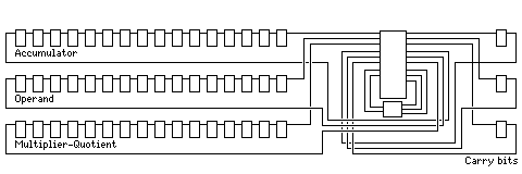
Some early computers used a type of arithmetic unit that involved the absolute minimum of arithmetic-related circuitry, a single full adder.
The diagram above illustrates the principle of a serial arithmetic unit. For a general arithmetic unit, able to perform multiplication and division directly as well as addition, three shift registers are required. Control logic routes bits shifted out of the least significant bits of the shift registers to the full adder which performs arithmetic, to flip-flops that retain carries between addition steps, and to an extra carry bit provided to each register.
Only a few early computers had serial arithmetic units. They were slower, since they broke arithmetic operations into many steps. As well, specifically because they increased the number of steps for each basic operation, they made the sequencing logic of the computers that used them more complex. This overhead tended to consume most of the savings realized through reducing the arithmetic unit to its bare minimum.
If, however, we take the buffer registers added to a dynamic RAM to increase its speed, and make them into the shift registers of a large number of serial arithmetic units, it appears to me that the serial arithmetic unit, rather than a parallel arithmetic unit, may serve very well.
Only a very small amount of logic, the routing gates and the full adder, are added to the memory chip in addition to the buffer registers which serve a useful purpose by speeding up the chip's normal function as a memory.
The sequencing logic, which is more complex, need be provided only once, in the central processing unit, which would then direct selected memory units, placed off-line as memory, to carry out the steps of large vector computations in parallel with conventional computations also being carried out by the central processor in conjunction with the remaining memory units.
The speed of a parallel computation is not impaired, as a function of the number of gates used, by using serial arithmetic units. To add two 64-bit words in a parallel fashion requires 64 full adders, but the time required, even with a fast adder design, is not the same as the time required for one full adder to add two bits and a carry, because of carry propagation. So, adding 64 pairs of numbers in parallel, by using 64 full adders separately, is actually faster than using a single parallel adder, built from the same amount of circuitry.
As well, since the steps within an operation are individually sequenced, additional flexibility is obtained. Serial arithmetic units can be used for functions such as the bit expand and compress operations of the BESM-6, for population count, and so on.
It is envisaged that the memory chips will have to have 64 data lines out, which increases their pin count. This is because it is expected that the most computationally intensive problems are those which involve 64-bit floating-point numbers. The flexibility of a serial arithmetic unit does permit using it for floating-point arithmetic, and this was done on the Ferranti Mercury computer.
The background computations would thus involve only very simple aligned operations between long vectors of numbers. One could, for example, multiply each element of a 4,096-element vector by the corresponding element of another 4,096-element vector located 32,768 words further up in memory. The computations would be of the SIMD type; therefore, the broadcast sequencing steps sent to the multiple serial arithmetic units would need to contain a provision for specifying that some steps are to be ignored depending on the value of a flip-flop within each arithmetic unit.
Note that a serial arithmetic unit contains three registers; and three is not a power of two. There are several ways to deal with this:
One could create serial arithmetic units from four buffer registers, thus making each unit more flexible. When the chip is used for memory, each buffer register is associated with a group of conventional memory locations by a single bus; when used to perform parallel arithmetic, the buses for four consecutive buffer registers are linked. The four linked buffer registers would be the ones associated with a group of four memory locations separated by N/4 in address, such as 0, N/4, N/2, and 3N/4, so that successive serial arithmetic units would operate on consecutive 64-bit storage elements.
One could have three layers of buffer registers, so that when the chip is used as a memory chip, it would have three fast windows into the conventional RAM.
One could have two layers of buffer registers, one of which provides a window into memory that is half the size of the window provided by the other layer. This could mean that the consecutive buffer registers in the larger layer would be connected to memory locations 0, 0+N, 0+2N, and so on, and then 1, 1+N, 1+2N, and so on, up to (N-1), (N-1)+N, (N-1)+2N and so on, while those in the smaller layer would be connected to memory locations 0, 0+N/2, 0+N, and so on, then 1, 1+N/2, 1+N, and so on, up to ((N/2)-1), ((N/2)-1)+N/2, ((N/2)-1)+N, and so on. In order to group these buffer registers in sets of three, what would happen, then, is that the buffer registers in the large group that were connected to locations 0 and 1 and those displaced by multiples of N from them would be grouped with the buffer register in the small group connected to location 0 and those displaced by multiples of N/2 from it, and then the buffer registers in the large group connected to locations 2 and 3 and those displaced by multiples of N from them would be grouped with the buffer register in the small group connected to location 1 and those displaced by multiples of N/2 from it, and so on.
The third alternative is particularly attractive, because it provides a path connecting memory locations 0 and 1 to location 0, locations 2 and 3 to location 1, 4 and 5 to location 2, and so on, which lends itself to performing Fast Fourier Transforms in the memory in the background. Note that the path from the smaller layer to conventional RAM would be the one applicable to most plain vector calculations, following the principles noted in the discussion of the first alternative.