Important Note: What is discussed on this page, unlike that which is described in the other pages of this portion of the web site, does not constitute part of the architecture these pages describe; it is present because it serves the main practical function of these pages, illustrating a broad range of concepts in computer architecture. |
The classic von Neumann stored-program computer architecture involves one central processor that does arithmetic, making use of information stored in a large memory. Thus, most of the information in the memory lies idle, while computations take place involving only a small number of items of data at a time.
Neural nets, cellular automata, and associative memories represent types of computing machines where the entire machine is engaged in computation. The trouble with these extreme solutions to the problem is that they are helpful only in certain specialized problem domains. On the other hand, a von Neumann computer with a magnetic drum memory or a magnetostrictive delay line memory is also using all its transistors (or vacuum tubes!), the potential building blocks of logic gates, to perform computation, so perhaps the wastefulness is merely the result of memory cells being comparable to logic gates in current integrated circuit technology.
A less extreme solution that has been suggested is building what is in effect a large parallel computer, composed of many small computers, each with a small memory, and, by providing shared access to those memories, use that large parallel computer as the memory of a large conventional computer with a large address space. One group working on this is the FlexRAM group, within the i-acoma group at the University of Illinois.
Historically, many computers had been built with quite small memories. A simple computer with only fixed-point operations on short words could have had a memory consisting of 4,096 words of 16 bits; a computer with hardware floating-point used to solve advanced mathematical problems could still have had a memory of only 32,768 words of 32 bits.
This doesn't really replace the von Neumann architecture with a new one. Even earlier computers, like the ENIAC, had only tiny memories, consisting of a few working numerical registers.
A massively-parallel computer that attempts to avoid the von Neumann bottleneck completely would, where a computer like the ENIAC would have made multiple passes over a long array of data, replace storing intermediate results in RAM with passing intermediate results along to the next computer. This is suitable to many types of problem, but if a step in a calculation requires, for example, access to a translate table, there is a problem. Even numerical problems which involve a three-dimensional array of points, each one interacting with its neighbors, require extra effort, but they can be handled, for example, by using a data stream consisting of 27 suitably offset copies of the array representing the space being simulated.
Because such a computer would be somewhat specialized, and not only is the von Neumann architecture what programmers are used to, but it is also more flexible in handling any type of problem, and because memory is no longer so expensive that having some of it lie idle is a critical problem (in a computer composed of many arithmetic/logic units and very little memory, often many of those arithmetic/logic units would lie idle), while having many little von Neumann computers does much less to force programmers into new ways of thinking, it still seems like a simpler and more practical alternative.
On the other hand, a dataflow architecture has one very great advantage over a conventional architecture for the problems which it can handle. As long as the number of steps in a calculation is less than the number of available ALUs, the computer will form an immense pipeline that will, after it produces the first result, continue producing results at the rate of one result in the time of a single elementary operation. In a more conventional parallel architecture, the temptation is strong, for simplicity in programming, to assign a long series of steps to one processor which could have been divided among several, thus limiting the overall speed of the calculation.
But even providing the modest degree of change, from one computer with a large, passive, memory to using memory that includes an internal processor every few kilobytes faces obstacles.
One obstacle to this is standardization. Another is whether this would be worth the effort. It is also not clear that simply because one can put sixteen megabytes of RAM on a chip, one can also put 2,048 microprocessors (one for each 4,096 16-bit words), or even 16 microprocessors (one for each 262,144 32-bit words), on that chip as well. Would these small microprocessors have to include hardware floating-point capability to be useful, or would smaller ones that can only do integer arithmetic on single bytes be appropriate?
One way to avoid making the wrong choice is not to make a choice. (Actually, of course, doing so is making a choice, and one that also can be wrong, but at least that is a third choice that might be overlooked, and which might be the best choice in some circumstances.) One could imagine a computer with a fractal organization: a handful of central processors that look like the one described here, designed to be as fast and powerful and possible, connected to a memory composed of chips containing 16 megabytes of RAM, 2,048 microprocessors that perform 16-bit addition, subtraction and logical operations, and perhaps 16 or perhaps 128 microprocessors that perform floating-point operations in hardware (using, respectively, either 32,768 or 262,144 32-bit words each). The memory on each chip would all be externally accessible, but in two separate contiguous chunks. In this way, the memory space containing the programs and local variables used by these internal microprocessors could be separated from the main data arrays, which would be more directly usable by the main computer as memory.
Each of the 2,048 fixed-point processors would have a memory of 8 Kbytes, divided into two areas of 1 Kbyte followed by one area of 2 Kbytes, followed by one area of 4 Kbytes.
Each of the 128 floating-point processors would have a memory of 128 Kbytes, and that memory would be the same memory as used by 16 fixed-point processors. The first 32 Kbytes of that memory would be composed of the second 2 Kbyte area from each fixed-point processor, the second 32 Kbytes of that memory would be the first 2 Kbyte area from each fixed-point processor, then the final 64 Kbytes of that memory would be the 4 Kbyte area from each fixed-point processor.
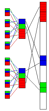
Externally, the chip would provide 16 megabytes, consisting first of the last 512 Kbytes of memory from each floating-point processor, and then the second 256 Kbytes of memory from each floating-point processor, and finally the first 256 Kbytes of memory from each floating-point processor. The chips would be organized into a memory such that the first 8 megabytes from all the chips would compose the first half of memory, the third 4 megabytes from all the chips would compose the third quarter of memory, and the fourth 4 megabytes from all the chips would compose the fourth quarter of memory.
What purpose would such an organization of memory, as illustrated in the diagram below, serve?
The area of memory shown in green, which is at the start of address space for the small fixed-point processors, would be considered to be largely their private preserve, containing program code and local variables. It would still be accessible by the other levels in the hierarchy, and thus the main computer would access it to provide those processors with their programs.
Similarly, the area shown in blue would be primarily the preserve of the small floating-point processors. Their programs and local variables would be there. They could also use any portion of the green area left unused by the fixed-point processors, or they could use any portion of the blue area the floating-point processor left unused.
The red area would be the area actively shared with the main computer. The main computer would reserve some memory space entirely for its own use; thus, either the first several auxilliary processors would perform computations involving only the areas shown in blue and green, or plain memory without auxilliary processors would be used for the first part of memory.
But in the later portions of the red area of outer memory, the auxilliary processors would access that memory, in a well-behaved manner, so that the outer processor would see a large contiguous array of memory upon the contents of which useful work was being done.
The intent is that a computer using active memory of this particular type would have a memory management unit that would behave as follows:
Given, in the slots dedicated to conventional memory, a 1 GByte memory module and a 256 MByte memory module, and in the slots dedicated to active memory, a 256 MByte memory module and a 64 MByte memory module, the central processor would be presented with a physical address space organized as follows:
00000000 Conventional 1 GByte module
3FFFFFFF
40000000 Conventional 256 MByte module
4FFFFFFF

80000000 Red area 256 MByte active module
87FFFFFF
88000000 Red area 64 MByte active module
89FFFFFF

90000000 Blue area 256 MByte active module
93FFFFFF
94000000 Blue area 64 MByte active module
94FFFFFF

98000000 Green area 256 MByte active module
9BFFFFFF
9C000000 Green area 64 MByte active module
9CFFFFFF
Thus, if the total amount of either conventional or active memory is not a power of two, the result would be that memory would be filled in a noncontiguous manner to a limited extent, but because active memory would still require special handling by the operating system, this would not be an obstacle to just slapping in more memory after the manner employed with present-day personal computers.
Also, some means of starting the auxilliary processors, and loading their program counters, would be needed; using an additional segment of address space for I/O ports for this purpose would probably be better than, say, causing the processors to react to external attempts to write to word 0 of their internal memory space, because there will no doubt be circumstances where all the memory, red, blue, and green, needs to be used by the main processor as memory, and no useful assistance can be rendered by the auxilliary processors.
Since an active memory component ought to be a standard item usable in different machines, it is important that it should be possible to select big-endian or little-endian operation. This will not raise any difficult architectural issues for these processors, unlike the case for the main computer architecture described here, since the internal processors, being designed to be simple, would not support unaligned memory accesses or packed decimal operations.
Of course, no gates would be wasted supporting more than one floating-point format; thus, the situation here is exactly the reverse of that which I propose for cache-internal parallel computing in the discussion of a hypothetical computer architecture of a conventional kind.
Also note that this concept could be generalized to a more deeply nested hierarchy of processors; two ways of doing so are illustrated in the following diagram:
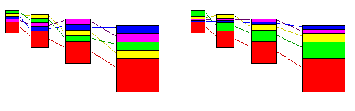
On the left is illustrated a simple way to generalize the principle to four layers; on the right, an alternative generalization to four layers of auxilliary processors is illustrated, in which the bottom layer of auxilliary processors, with a small amount of address space each, still have one-fourth of that space as their reserved program area, but the processors at the next higher level, with a larger available address space, only recieve one-eighth of that larger space for their programs, and the processors at the two highest levels recieve only one-sixteenth of their even larger address space for their programs. In practice, three layers of auxilliary processors are about as much as would be realistic; organizing them according to this alternative principle, but omitting the highest level, would give the top two layers one-eighth of their address space for their programs.
The first arrangement is oriented towards a number of layers which is a power of two, while the second arrangement retains its structure with any number of layers. It is possible to combine the two principles shown to create, for example, an arrangement in which the proportion of private memory used by processors in each layer, except for the topmost two layers, is halved every two layers instead of the same for all layers (as in the first arrangement) or halved for each layer except the topmost (as in the second arrangement).
The notion of having an active memory in which a processor is associated with each limited expanse within memory as a method of achieving a high level of parallelism has been around for some time; I am fairly certain that the idea of taking this to multiple layers has also been advanced, and it would not surprise me if even the specific memory mapping proposal advanced here, bizarre though it may seem, had been previously described in the literature.
The use of multiple processors whose program storage is at repeated locations in memory brings to mind another architectural innovation that might be extremely useful even in connection with conventional memory. If it were possible, in effect, during a write to memory, to set certain address lines to a "Don't Care" state, so that the value output on the data lines was written to all locations whose addresses matched those of the address bits which are specified, this would speed up certain types of operation immensely. It might be necessary to exclude some of the least significant bits of the address from this capability, but this seems to demand much less additional circuitry, compared to conventional memory, than associative memory, for example.
What would the individual processors look like? As they should be constructed using a bare minimum number of gates, I envisage that the auxilliary processors on the lowest levels would only have accumulators and not general registers, although even the small integer processor would have an index register, since that would be an asset in processing character strings. Thus, the design at least of the computers at the two lowest levels in the hierarchy would resemble that of the earliest computers.
What would these component computers look like?
The smallest computers in the hierarchy, with an address space of 8 Kbytes organized as 4,096 halfwords, might have an instruction set like the following:
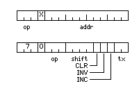
The following memory-reference instructions would be defined:
000 JMP Jump
001 JPS Jump to Subroutine
010 ADD Add to accumulator
011 AND AND with accumulator
100 LDA Load Accumulator
101 STO Store accumulator
110 DSZ Decrement and Skip if Zero
If the X bit is set, the contents of the index register are added to the address field before it is used.
The Jump to Subroutine instruction treats the last thirteen bits of the word at the effective address as if they were the last thirteen bits of a store instruction, except that what is being stored is not the contents of the accumulator, but a value one greater than the address of the Jump to Subroutine instruction itself; and then it transfers control to the location following that word.
Note that because the opcode of the jump instruction is zero, the stored return address also serves as a jump instruction to perform the return from the subroutine.
Where the opcode field is 7, instead of a memory-reference instruction, we have an operate instruction.
The op field has the following interpretation:
000 no operation
001 SHL   Shift left
010 ASR   Arithmetic shift right
011 LSR   Logical shift right
100 RAL   Rotate accumulator left
101 RLC   Rotate left through carry
110 conditional skip
111 conditional skip with carry test
In the case of a conditional skip, instead of the shift field indicating the number of places to shift, its first three places indicate the type of test to perform:
000 no operation
001 SPL   Skip if plus
010 SZE   Skip if zero
011 SPZ   Skip if positive or zero
100 SNE   Skip if negative
101 SNZ   Skip if not zero
110 SMZ   Skip if minus or zero
111 SKP   Skip unconditionally
and in the case of a conditional skip with carry test, the first three places in the shift field indicate the following tests:
000 no operation
001 SKC   Skip if carry
010 SNC   Skip if no carry
011 SKP   Skip unconditionally
101 SCH   Skip if carry and not negative
110 STN   Skip if no carry and negative
111 SKV   Skip if carry and not negative,
           or no carry and negative
In the case where the op field indicates no operation, or either of the two forms of conditional skip, the last place in the shift field, if a one, indicates the following operation:
CLC Clear carry
The following operations:
CLR Clear accumulator
INV Invert the bits of the accumulator
INC Increment the accumulator
are each controlled by individual bits of the instruction. If both the INV and INC bits are set, one gets the instruction:
NEG Two's complement the accumulator
The tx field has the following interpretation:
00 no operation
01 LXA   Load index from accumulator
10 LAX   Load accumulator from index
11 XAX   Exchange accumulator and index
The operations described in the word are performed in this order:
Thus, one can combine CLA with XAX to retrieve and clear the index register, or one can combine CLA with a conditional skip instruction to erase the accumulator after it has been tested.
Of course, this design is strongly influenced by that of the Digital Equipment Corporation's PDP-8 computer and other similar machines.
A possible instruction set for a processor with floating-point capability which addresses a span of 32,768 words each 32-bits long could involve the following instruction formats:
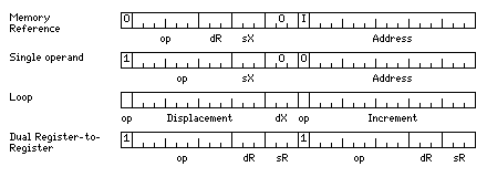
and the following instructions:
0xxxxx 0xxxxx SAXSP  Signed Add to Index and Skip if Past
0xxxxx 1xxxxx IXBLE  Increment Index and Branch if Low or Equal
1xxxxx 0xxxxx SAXJ   Signed Add to Index and Jump

001xx0 xxxxxx CAS    Compare and Skip
002xx0 xxxxxx L      Load
003xx0 xxxxxx ST     Store
004xx0 xxxxxx A      Add
005xx0 xxxxxx S      Subtract
006xx0 xxxxxx M      Multiply
007xx0 xxxxxx D      Divide

014xx0 xxxxxx N      AND
015xx0 xxxxxx O      OR
016xx0 xxxxxx X      XOR

021xx0 xxxxxx CASF   Compare and Skip Floating
022xx0 xxxxxx LF     Load Floating
023xx0 xxxxxx STF    Store Floating
024xx0 xxxxxx AF     Add Floating
025xx0 xxxxxx SF     Subtract Floating
026xx0 xxxxxx MF     Multiply Floating
027xx0 xxxxxx DF     Divide Floating

031xx0 xxxxxx CASD   Compare and Skip Double
032xx0 xxxxxx LD     Load Double
033xx0 xxxxxx STD    Store Double
034xx0 xxxxxx AD     Add Double
035xx0 xxxxxx SD     Subtract Double
036xx0 xxxxxx MD     Multiply Double
037xx0 xxxxxx DD     Divide Double

042xx0 xxxxxx LX     Load Index
043xx0 xxxxxx SX     Store Index

050xx0 xxxxxx JMS    Jump to Subroutine

060xx0 xxxxxx JMP    Jump

06xxx0 xxxxxx conditional jump
This architecture draws on both the IBM 7094 computer and the Control Data 6600 computer for inspiration.
Note that the loop instructions are distinguished from the other instructions having the same bits in the two bits functioning as opcode bits for loop instructions by always having a nonzero value in the dX field.
The SAXSP instruction takes the quantity in the Displacement field to be a signed integer from -2,048 to 2,047, and adds that to the contents of index register indicated in the dR field. The result becomes the new contents of that index register. It is compared to the quantity in the Increment field, which is treated as an unsigned integer from 0 to 32,797. When the Displacement field is positive, if the new contents of the index register are greater than the value in the Increment field, the next instruction is skipped. When the Displacement field is negative, if the new contents of the index register are less than or equal to the number in the increment field, the next instruction is skipped.
Here, the Displacement field functions as the increment, and the Increment field functions as the limit.
The IXBLE instruction increments the index register indicated in the dR field. If the result is less than or equal to the quantity in the Increment field, then the unsigned value, from 0 to 4,095, in the Displacement field is subtracted from the address of the IXBLE instruction to form the address to which control is to be transferred.
Once again, the Increment field is used as a limit, but the Displacement field is indeed a branch displacement.
The SAXJ instruction takes the quantity in the Increment field to be a signed integer from -16,384 to 16,383 and adds it to the contents of the index register indicated by the dR field, with the result replacing the former contents of that index register. Then control is transferred to the address indicated by subtracting the unsigned value in the Displacement field from the address of the SAXJ instruction itself.
Each of these three instructions can be used to assist in coding program loops, where an index register is used as the loop counter, but in different ways. The SAXSP instruction can be combined with a jump instruction to form a general counter loop. The SAXJ instruction can be combined with a separate test for the condition for the end of the loop. When the loop involves the counter being stepped by one, the IXBLE instruction provides all the necessary logic for the loop by itself.
The Jump to Subroutine instruction stores the return address at the location pointed to by the last 15 bits of the 32-bit word that is at its effective address, and then transfers control to the word following. It ignores the indirect bit, if that is set in that word, interpreted as an instruction; thus, if that word is an indirect Jump instruction, transferring control using a normal Jump instruction to the first word of a subroutine will effect a return from the subroutine.
The Compare and Skip instructions transfer control to the next word if the target is less than the contents of the accumulator, to the word after the next if they are equal, and causes two 32-bit words to be skipped if the target is greater.
In a three-level hierarchy of processors, in addition to having a processor like the above every eight kilobytes, and having a simple processor with floating-point capabilities every one hundred and twenty-eight kilobytes, thus having sixteen of the next smaller computers below it, one could have another simple processor with floating-point capabilities and a memory consisting of 262,144 words of memory, each 32 bits long, or one megabyte, each having eight of the next smaller processor below it, or one could have a microprocessor with a more currently conventional instruction set every sixteen megabytes, which would have 128 of the next smaller processor below it. Or one could have both, for a four-level hierarchy.
One possible instruction set for the more conventional microprocessor with an address space of sixteen megabytes would be the one described here, but omitting at least the long vector registers, the long vector scratchpad, register renaming, and the ability to have multiple threads running concurrently. The supplementary registers, the extended translate instruction, the additional instructions available in the extended operate modes, and even the short vector registers would be additional candidates for omission.
The smaller computers would be designed to require a minimal number of gates, and so they would not be designed to be faster than the available memory. As they are sharing the same memory, time would have to be allocated between them. In a hierarchy with two levels of auxilliary processors, memory cycles might be allocated like this:
main processor
32-bit auxilliary processor
main processor
16-bit auxilliary processor
If the internal bus of the memory was 32 bits wide instead of 16 bits wide, instead of the auxilliary processors each operating on 4,096 contiguous 16-bit words as seen by the auxilliary processors operating on 32,768 32-bit words, they would be more efficiently organized in pairs, one member of each pair working on left halves, one member on right halves.
Similarly, if the main processor had a 256-bit data bus, and accessed the memory with 16-way interleaving, instead of the processors operating on 32,768 32-bit words acting on a contiguous area of the main processor's memory, 32-bit areas in that memory could be divided between 128 of these processors in rotation at a time.
While that would be the most efficient organization, it would complicate transferring data between processors at different levels of the hierarchy. The 32-bit processors would be more useful to the main processor if they could operate directly on small arrays as seen by the main processor.
Also, note that the processors at lower levels are not given any way of communicating with each other directly, and thus any required interprocessor communication ties up the processors at higher levels.