The idea of replacing an essentially passive array of memory elements by one that is peppered with processors for every so much memory is one that has been proposed many times, but one that has seldom been implemented. It has been considered visionary rather than practical.
On the other hand, banks of arithmetic-logic units set up to perform calculations in parallel have been implented many times, and have been in use for some time.
A limited amount of vector arithmetic capability had been present in some computers using vacuum tubes (the AN/FSQ-7) or transistors (the TX-2 and the AN/FSQ-32), of a type resembling the MMX feature available with Intel microprocessors or the short vector instructions on the architecture described here.
Many of the early machines which provided long vector capabilities did so through a special rapid pipelining mode rather than by having multiple arithmetic-logic units, one for each element of a vector or at least each element of a sizable chunk of a vector.
It was still obvious from the start that a vector unit should ideally connected to memory along a data path having the same width in bits as the combined width of the arithmetic units involved.
In order that the position on this wide data bus of each arithmetic unit be fixed, it would appear preferable to organize an external vector unit of this type along the lines of that performing the short vector instructions of the main processor architecture we have been examining, rather than along the lines of that performing the long vector instructions. However, historically, external vector units have tended to be organized with a fixed number of arithmetic-logic units, so that when doing double-precision arithmetic, half the arithmetic-logic units, even if they are ones only capable of single-precision arithmetic, would not be idle. This can be minimized by making the ALU reconfigurable, so that much of the same logic is used whether one long or two short operands are being worked on, but some circuitry (such as that for normalization) will unavoidably be idle in the case of fewer operands.
In addition to supercomputers with vector capabilities, later vector floating-point units were available as third-party add-on systems for both mainframes and minicomputers from companies such as Floating Point Systems.
More recently, IBM's Enterprise Systems Architecture/390 provided for an optional external vector arithmetic unit the internal width of which would vary from one model to another, but which shared a common interface from the programmer's perspective. This vector facility connected directly to the CPU, and, at least in the case of the version used with ES/9000, operated on data in cache. It had internal vector registers, so it provided a basic architecture similar to that of vector supercomputers like the Cray-1 and its successors. Before that, add-on vector units offered for the System/360 and the original System/370, such as the IBM 2938 Array Processor and the IBM 3838 Array Processor, had their own internal memories, to which data would be transferred before the start of a computation involving vectors.
In the context of the specific architecture being presented here on these pages, it may be noted that the vector mode and the short page mode of operation provide memory-to-memory vector operations only, and the modes which provide access to the internal long vector registers also include memory-to-memory vector operations. Circuitry to detect the presence of an appropriate external coprocessor, and to permit the delegation of these operations to that coprocessor, can be added to the design without in any way altering the instructions themselves. However, if an external vector coprocessor were present, it would be useful to have available vector instructions which had a length field which was 16 or even 32 bits in length, instead of only six bits in length, so that a single instruction could cause a long vector to be processed concurrently with normal machine operations. Of course, the external vector coprocessing units would be pipelined, as this is an inexpensive method of permitting them to perform a larger number of operations in a given time.
Since the external vector coprocessing system would be connected directly to main memory, it always treats memory as divided into 32-bit words of the normal size, ignoring any use of 36-bit, 24-bit, 40-bit or 60-bit words by the central processor, and it also does not handle floating-point numbers of the Medium type, but instead provides support for floating-point numbers of the Small type, just as is done by the Short Vector arithmetic unit.
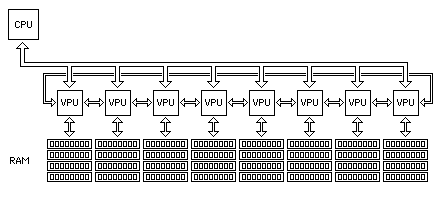
The following illustration depicts the architecture for external vector coprocessing that is envisaged as being associated with the processor architecture described here, as will be discussed below:
Because the external vector coprocessing system could consist of a multiplicity of functional units, such as, for example, a set of sixteen identical chips, and since it works with operands in memory rather than the cache, it would have a wide path to memory. This suggests the possibility of a design in which the external vector coprocessing chips also perform a memory interface function; thus, while the main microprocessor could have, as given as an example, a 256 bit wide data bus, each of sixteen vector coprocessing units could have a data bus to memory of similar width, as well as being connected to the processor data bus, which could then operate at a higher speed than that of the memory.
However, if it is not possible to have a processor data bus that runs more quickly than the bus that can be used with the memory, then a different architecture would be more appropriate:
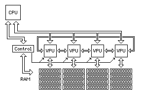
Here, instead of the chips just being memory controllers in addition to containing external vector processing units, they would also contain external L3 cache. This still serves a useful purpose, as external DRAM has latency limitations in addition to that imposed by the speed of the external data bus being slower than the processor cycle time. Four of these chips, instead of eight, are shown in this diagram, since each of those chips would supply 64 out of the 256 bits of the processor data bus; this way, double-precision floating-point numbers would stay in one piece inside each of them.
This also indicates that the individual chips in that system, having a fixed-width path to memory, would likely work on a principle similar to that of the ALU used for the short vector instructions.
Also, while an elaborate bus structure was shown on this page for allowing, in two steps, vector operands beginning at any arbitrary position to be brought into alignment, for the case of an elaborate implementation of the architecture having a set of 64 ALUs within the chip itself, for the external system, such a capability is unlikely. Instead, if the external system consists of a row of chips, each one coupled to a bank of memory, likely each chip would simply be connected to its two immediately adjacent neighbors. This, of course, would mean that vectors not fully aligned, in terms of the width of the entire assembly of external coprocessor chips, would involve a significant performance penalty, although even that penalty would not outweigh the benefit of avoiding the limited-width data path to the CPU itself.
Note also that the bus between the RAM and each VPU would be able to handle data more quickly than the access time of the RAM, and, thus, the RAM would still be interleaved in this configuration; that would combine with the wider path to memory provided by the multiple vector processor units to further improve memory bandwidth. Essentially, the memory is interleaved because it is slower than the speed of a conventional data bus, and with the vector processing units, multiple conventional data buses are present, each one connecting one of those units to a slice of memory, and a high-speed data bus is provided to the main CPU.
Modern memory modules, used in today's personal computers, include on-chip interleaving of memory banks for higher data transfer speeds. Two-way interleaving appeared first, and more recently, four-way interleaving has made an appearance. Even before this happened, of course, high-performance computers could implement interleaving with external circuitry and by requiring that memory modules be installed in matched sets.
Let us suppose that, in a high-performance implementation, interleaving was taken to what may seem to be an extreme; let the memory be 16-way interleaved, and, in addition, eight of these combination vector coprocessor and memory management chips are used, for a bus to main memory that is 2,048 bits wide. This would mean that the speed at which data is fed to the CPU chip, through its 256-bit external data bus, would be 128 times the basic speed at which data is available from the memory cells used in the main memory.
Using the high-performance chip architecture given here as an example implementation, it takes sixteen fetches of 256 bits of data to fill a single cache line, each cache line being 4,096 bits wide, in order to provide 64 vector arithmetic-logic units each with 64 bits of data in parallel. Thus, even with all this effort being taken to provide data to the processor at a high speed, external data streamed to the chip at the maximum possible rate would only match the rate at which data could be fetched internally from the cache if the memory cells of the cache were but eight times faster than the memory cells used in main memory.
Due to latencies and other issues, the cache would still justify its existence if the disparity in speeds were only eightfold, but it is likely that the disparity will be larger than that.
These instructions have the form:
The length field must be a multiple of 32 bytes, which means its last five bits must be zero, as it is in units of bytes, and all operands must be aligned on a 32 byte, or 256 bit, boundary.
These instructions are available from normal mode, scratchpad mode, and compact mode. As well, they are available from simple mode, with their first 16 bits modified as follows:
Normal
Compact Simple
------- ------
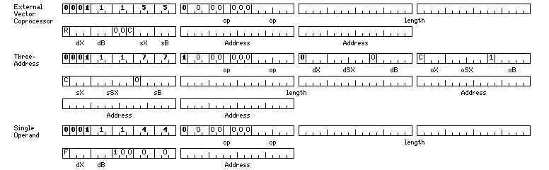
External Vector Coprocessor 011155 051550
Three-Address 011177 051770
Single Operand 011144 051440
Their opcodes are:
011155 000004 XVAB      External Vector Add Byte
011155 000005 XVSB      External Vector Subtract Byte

011155 000013 XVMVSM    External Vector Move Small

011155 000016 XVMINB    External Vector Minimum Byte
011155 000017 XVMAXB    External Vector Maximum Byte

011155 000024 XVAH      External Vector Add Halfword
011155 000025 XVSH      External Vector Subtract Halfword
011155 000026 XVMH      External Vector Multiply Halfword
011155 000027 XVDH      External Vector Divide Halfword

011155 000033 XVMVF     External Vector Move Floating

011155 000036 XVMINH    External Vector Minimum Halfword
011155 000037 XVMAXH    External Vector Maximum Halfword

011155 000044 XVA       External Vector Add
011155 000045 XVS       External Vector Subtract
011155 000046 XVM       External Vector Multiply
011155 000047 XVD       External Vector Divide

011155 000052 XVMV      External Vector Move
011155 000053 XVMVD     External Vector Move Double
011155 000054 XVN       External Vector AND
011155 000055 XVO       External Vector OR
011155 000056 XVMINH    External Vector Minimum
011155 000057 XVMAXH    External Vector Maximum

011155 000064 XVAL      External Vector Add Long
011155 000065 XVSL      External Vector Subtract Long
011155 000066 XVML      External Vector Multiply Long
011155 000067 XVDL      External Vector Divide Long

011155 000073 XVMVQ     External Vector Move Quad
011155 000074 XVSW      External Vector Swap
011155 000075 XVX       External Vector XOR
011155 000076 XVMINH    External Vector Minimum Long
011155 000077 XVMAXH    External Vector Maximum Long

011155 001004 XVASM     External Vector Add Small
011155 001005 XVSSM     External Vector Subtract Small
011155 001006 XVMSM     External Vector Multiply Small
011155 001007 XVMSM     External Vector Divide Small

011155 001012 XVMINSM   External Vector Minimum Small
011155 001013 XVMAXSM   External Vector Maximum Small

011155 001024 XVAF      External Vector Add Floating
011155 001025 XVSF      External Vector Subtract Floating
011155 001026 XVMF      External Vector Multiply Floating
011155 001027 XVDF      External Vector Divide Floating

011155 001032 XVMINF    External Vector Minimum Floating
011155 001033 XVMAXF    External Vector Maximum Floating
011155 001034 XVAU      External Vector Add Unnormalized
011155 001035 XVSU      External Vector Subtract Unnormalized
011155 001036 XVMU      External Vector Multiply Unnormalized
011155 001037 XVDU      External Vector Divide Unnormalized

011155 001044 XVAD      External Vector Add Double
011155 001045 XVSD      External Vector Subtract Double
011155 001046 XVMD      External Vector Multiply Double
011155 001047 XVDD      External Vector Divide Double

011155 001052 XVMINF    External Vector Minimum Double
011155 001053 XVMAXF    External Vector Maximum Double
011155 001054 XVAUD     External Vector Add Unnormalized Double
011155 001055 XVSUD     External Vector Subtract Unnormalized Double
011155 001056 XVMUD     External Vector Multiply Unnormalized Double
011155 001057 XVDUD     External Vector Divide Unnormalized Double

011155 001064 XVAQ      External Vector Add Quad
011155 001065 XVSQ      External Vector Subtract Quad
011155 001066 XVMQ      External Vector Multiply Quad
011155 001067 XVDQ      External Vector Divide Quad

011155 001072 XVMINQ    External Vector Minimum Quad
011155 001073 XVMAXQ    External Vector Maximum Quad
011155 001074 XVAUQ     External Vector Add Unnormalized Quad
011155 001075 XVSUQ     External Vector Subtract Unnormalized Quad
011155 001076 XVMUQ     External Vector Multiply Unnormalized Quad
011155 001077 XVDUQ     External Vector Divide Unnormalized Quad
and the C bit in the instruction indicates the source operand is a single variable instead of a vector, and the R bit indicates that the destination is to be subtracted from the source, with the result going in the destination, or the source is to be divided by the destination with the result going in the destination. For constant operations, the mnemonics in these cases end in C (Constant) or RC (Reversed Constant) respectively.
The MIN instruction returns the lesser of its two arguments, the MAX instruction returns the greater of its two arguments; just like the ZIN single-operand instruction, to be described below, this helps in performing more sophisticated operations on external vectors without the need for conditional branches on individual elements. This is a technique used in graphics processors; in the main CPU, this problem is dealt with in a different fashion, using mask bits and multi-way vector instructions.
Three-address instructions, in which either the source operand or the operand operand may be constants, but which do not need, and do not have, the option of a reversed direction, are also present.
Note that unnormalized floating-point operations are included; this is important so that it is possible to keep track of significance in what may be an enormous computation.
The single-operand instruction format shows a seven-bit field as available for the opcode. This opcode field is similar to a concatenation of the two-bit type field, and the five-bit opcode field, in a normal floating-point single-operand instruction, but the values of the five-bit opcode field are modified to avoid conflicts between these opcodes and some opcodes that are reserved for special purposes from those used for two-address and three-address instructions; they must also be reserved here, since whether an instruction is a single-address instruction, a two-address instruction, or a three-address instruction, is not indicated until after the first halfword of the instruction.
The opcodes for external vector single-operand instructions are:
011144 000001 XVSINSM  011144 000041 XVSIN    011144 001001 XVSIND   011144 001041 XVSINQ
011144 000002 XVCOSSM  011144 000042 XVCOS    011144 001002 XVCOSD   011144 001042 XVCOSQ
011144 000003 XVTANSM  011144 000043 XVTAN    011144 001003 XVTAND   011144 001043 XVTANQ
011144 000004 XVRSQSM  011144 000044 XVRSQ    011144 001004 XVRSQD   011144 001044 XVRSQQ
011144 000005 XVASNSM  011144 000045 XVASN    011144 001005 XVASND   011144 001045 XVASNQ
011144 000006 XVACSSM  011144 000046 XVACS    011144 001006 XVACSD   011144 001046 XVACSQ
011144 000007 XVATNSM  011144 000047 XVATN    011144 001007 XVATND   011144 001047 XVATNQ

011144 000011 XVSINHSM 011144 000051 XVSINH   011144 001011 XVSINHD  011144 001051 XVSINHQ
011144 000012 XVCOSHSM 011144 000052 XVCOSH   011144 001012 XVCOSHD  011144 001052 XVCOSHQ
011144 000013 XVTANHSM 011144 000053 XVTANH   011144 001013 XVTANHD  011144 001053 XVTANHQ
011144 000014 XVRECSM  011144 000054 XVREC    011144 001014 XVRECD   011144 001054 XVRECQ
011144 000015 XVASNHSM 011144 000055 XVASNH   011144 001015 XVASNHD  011144 001055 XVASNHQ
011144 000016 XVACSHSM 011144 000056 XVACSH   011144 001016 XVACSHD  011144 001056 XVACSHQ
011144 000017 XVATNHSM 011144 000057 XVATNH   011144 001017 XVATNHD  011144 001057 XVATNHQ

                                              011144 001021 XVCLR    011144 001061 XVINV
011144 000022 XVZINB   011144 000062 XVZINH   011144 001022 XVZIN    011144 001062 XVZINL
011144 000023 XVABSB   011144 000063 XVABSH   011144 001023 XVABS    011144 001063 XVABSL
011144 000024 XVSQRSM  011144 000064 XVSQR    011144 001024 XVSQRD   011144 001064 XVSQRQ
011144 000025 XVQBRSM  011144 000065 XVQBR    011144 001025 XVQBRD   011144 001065 XVQBRQ
011144 000026 XVLOGSM  011144 000066 XVLOG    011144 001026 XVLOGD   011144 001066 XVLOGQ
011144 000027 XVEXPSM  011144 000067 XVEXP    011144 001027 XVEXPD   011144 001067 XVEXPQ

011144 000031 XVZINSM  011144 000071 XVZINF   011144 001031 XVZIND   011144 001071 XVZINQ
011144 000032 XVSGNB   011144 000072 XVSGNH   011144 001032 XVSGN    011144 001072 XVSGNL
011144 000033 XVNEGB   011144 000073 XVNEGH   011144 001033 XVNEGD   011144 001073 XVNEGL
011144 000034 XVCLRSM  011144 000074 XVCLRF   011144 001034 XVCLRD   011144 001074 XVCLRQ
011144 000035 XVABSSM  011144 000075 XVABSF   011144 001035 XVABSD   011144 001075 XVABSQ
011144 000036 XVSGNSM  011144 000076 XVSGNF   011144 001036 XVSGND   011144 001076 XVSGNQ
011144 000037 XVNEGSM  011144 000077 XVNEGF   011144 001037 XVNEGD   011144 001077 XVNEGQ
The additional opcodes that may be unfamiliar here are RSQ, which calculates the reciprocal of the square root, ZIN, which replaces its argument by zero if it is negative, and REC, which calculates the reciprocal. Note also the presence of a few fixed-point single operand instructions, fixed-point forms of CLR, ABS, SGN, NEG, and ZIN, as well as INV, which performs a one's complement. Also note that XVINV is distinguished by XVCLR by type bits rather than opcode bits (as was also done for the AND and Swap instructions, and the OR and XOR instructions to make room for the floating-point move instructions), so that opcode space is available for the fixed-point XVZIN instructions.
The diagram below:
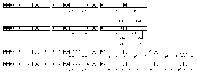
illustrates the instruction formats associated with the external vector opcodes which end in three zero bits, which were unused up to this point. As with the other instructions, in the case of advanced compound mode, the 123400 prefix halfword is added. These opcodes are followed by the additional instruction halfwords as shown in the diagrams above, and then the length field (omitted within a stretch, as described below) and the other addressing fields of normal two-address and three-address external vector memory-reference instructions which vary depending on the mode of operation in effect.
Because the positions of later halfwords in the instruction are changed, although the bits in them which indicate whether an instruction is a two-address or a three-address instruction should still be set to their appropriate values, as shown above for the different instruction modes, the first bit of the halfword immediately following the opcode also indicates, if 0, that the instruction is a two-address instruction, and, if 1, that the instruction is a three-address instruction.
These multiple-component instructions treat vectors as composed of repeated groups of two (as illustrated in the first two formats in the diagram above) or four (in the case of the last two formats in the diagram above) numbers.
In a two-address instruction, the values for op1, op2, op3 and op4 have the following meanings:
0010 MOV

0100 ADD
0101 SUB
0110 MUL
0111 DIV

1011 XOR
1100 AND  ADDU
1101 OR   SUBU
1110      MULU
1111      DIVU
and in a three-address instruction, the values for op1, op2, op3 and op4 have the following meanings:
000 ADD
001 SUB
010 MUL
011 DIV
100 AND  ADDU
101 OR   SUBU
110      MULU
111 XOR  DIVU
the ones in the second column replacing the logical operations for floating-point numbers with unnormalized floating-point arithmetic.
In a two-component instruction, operations are performed on pairs of numbers of the type indicated in the first halfword of the instruction. For each component in the result, an operation is indicated, and a source component is indicated, and, if it is a three-address instruction, an operand component is also indicated. All possible destination components are used; the destination component of the operation indicated by op1 is the first of the two destination components, and the destination component of the operation indicated by op2 is the second of two destination components.
In a three-address instruction, there is also a two-bit op field; this indicates how the result of the operation performed on the source component and the operand component is applied to the destination component. The possible values for this field are:
00 replace
01 zero and subtract
10 add
11 subtract
Thus, it is possible to divide the contents of the operand field by the contents of the source field, and then subtract the result from the contents of the destination field, with the result being placed in the destination field.
With two two-component instructions, it is possible to multiply two vectors of complex numbers.
In a four-component instruction, we again have a series of four instructions which select a source component, and, in a three-address instruction, an operand component, within the corresponding elements of the source vector and the operand vector of the instruction.
This type of instruction is very similar to, but is a superset of, the type of operation commonly found in pixel (or fragment) and vertex shaders in graphics chips. However, tasks such as the rasterization of polygons still require either a conventional software program, or the use of a conventional special-purpose graphics chip.
Also note that if the external vector coprocessors have a 256-bit path to memory, four-component operations on the Quad floating-point type are not possible unless pairs of external vector coprocessors co-operate in performing them. Narrower paths to main memory could impose more severe restrictions.
In many cases, an alternative to using multiple-component instructions would be to use multiple vectors, each vector being of one component. This requires more instructions, but that is not a real cost if the length of a vector handled by an instruction is bounded with sufficient severity that it is shorter than the actual length of the arrays on which operations are being performed. With a 32-bit length for vectors, this is not the case for the external vector coprocessor. The use of long vector instructions with stride is also possible for conversion between the two possible memory organizations.
Because the operands of these instructions have a length indicated by a thirty-two bit length field, it is not practical for the external coprocessor units to posess registers of sufficient size to store a complete operand. However, the ability to use registers, so that not every step in a calculation requires a memory access, is very important. This is handled by providing a special interpretation to the following opcodes for the two-address form of an external vector operation:
011244 000002 XVLB   External Vector Load Byte
011244 000003 XVSTB  External Vector Store Byte

011244 000022 XVLH   External Vector Load Halfword
011244 000023 XVSTH  External Vector Store Halfword

011244 000042 XVL    External Vector Load
011244 000043 XVST   External Vector Store

011244 000062 XVLL   External Vector Load Long
011244 000063 XVSTL  External Vector Store Long

011244 001002 XVLSM  External Vector Load Small
011244 001003 XVSTSM External Vector Store Small

011244 001022 XVLF   External Vector Load Floating
011244 001023 XVSTF  External Vector Store Floating

011244 001042 XVLD   External Vector Load Double
011244 001043 XVSTD  External Vector Store Double

011244 001062 XVLQ   External Vector Load Quad
011244 001063 XVSTQ  External Vector Store Quad
These are memory-to-register instructions. The dX field instead serves as a dR field, and the halfword containing the corresponding address (or, in the case of the short page modes, the indirect bit, the dB field, and the address) is omitted from the instruction, because the destination is a register, and is not in memory; the halfword containing the source address remains present in the instruction. The store instruction also omits the length specification.
A load instruction begins a stretch of code using registers, and a store instruction ends a stretch of code using registers.
The stretch should be treated as if it were a single instruction; no attempt should be made to branch into it, or out of it. For one thing, an attempt to branch into a stretch from instructions not part of a stretch would result in the instructions within it not being interpreted correctly, because the format of instructions is being changed by the omission of the length field. A stretch should be thought of as being similar to a series of instructions within an FLL (Fixed-Length Loop) instruction, since the series is sent once to the external vector coprocessors, but is performed repeatedly by them, as many times as the width of their path to memory lies within the length specification of the initial load instruction.
The length specification in the load instruction applies to all the instructions in the stretch. A stretch consists exclusively of memory-reference instructions and single-operand instructions, both fixed and floating. The multiple-component instructions are allowed within a stretch. All these instructions will be treated as external vector instructions; register references will be to the internal registers of the external vector coprocessor.
These registers will be as wide as the bus connecting each external vector coprocessor to memory; the instructions making up the stretch will be repeated, therefore, with a suitable displacement each time, until the entire length of the vector is processed. Thus, none of the vectors referenced in memory may overlap, or the results will be unpredictable.
Also, within a stretch, the opcode 011144 000021 will be used as an instruction prefix, to indicate that the source operand of an instruction is a scalar, to be used as a constant operand acting on every element of a vector.
In addressing modes that provide three-address memory-to-memory scalar operations, they may be used; otherwise, a three-address external vector instruction with the length field omitted may be present within a stretch as well. Register operands are specified by using a zero base register value in the vector register and symmetric vector register modes, as well as in the conventional modes; in the short page modes, the three bits following the index register field, normally zero, are to contain the bits 111 to indicate a register operand.
Since a load instruction begins a stretch, and a store instruction ends a stretch, transfers within the stretch between registers and memory are handled by the following instructions:
011177 000012 XVMVB     External Vector Move Byte
011177 000032 XVMVH     External Vector Move Halfword
011177 000052 XVMV      External Vector Move
011177 000072 XVMVL     External Vector Move Long

011177 000013 XVMVSM    External Vector Move Small
011177 000033 XVMVF     External Vector Move Floating
011177 000053 XVMVD     External Vector Move Double
011177 000073 XVMVQ     External Vector Move Quad
Note that, due to a lack of available opcodes, the move instructions for the floating-point types are grouped with fixed-point opcodes.
Only a limited subset of the available floating-point formats supported by the architecture would be available by means of vector coprocessor operations. It is not yet defined how the format to use would be specified, if any choice at all is made available. Presumably, a limited-width field in the Program Status Block would contain the external vector coprocessor floating-point format in current use, which would be signalled to the external vector coprocessor each time an operation is requested.
It is envisaged that in any case, the Standard floating-point format would be supported, since the IEEE 754 floating-point format has become the standard floating-point format supported by virtually all microprocessors. As a second choice, the Compatible or Modified formats, for compatibility with the IBM System/360 series of computers and their successors, suggest themselves. But another very important alternative format would be the Common floating-point format. This is the floating-point format used when it is desired to increase the total floating-point performance of the central processing unit to its maximum value by modifying Simple Floating-Point operation, which is carried out by the fixed-point arithmetic units, by decreasing the length of the exponent field, so that compatibility with the floating-point arithmetic units is achieved. Allowing the external vector coprocessing units to handle this format as well permits all available floating-point processing capacity to use the same floating-point format to maximize floating-point throughput.
Since the external vector coprocessor only works with memory in its native width, the only variation of the Common floating-point format that would be used would be the one where an excess-128 binary exponent occupied the last eight bits of a 32, 64, or 128 bit long floating-point number with a sign-magnitude mantissa. Note also that the integer arithmetic units of the central processing unit do not provide the guard, round, and sticky bits, or their equivalents, that both the central processing unit floating-point units and the external vector coprocessor provide, and, thus, there is a penalty in accuracy for maximizing floating-point performance in this manner.