It has been possible to include instructions making use of advanced capabilities of this architecture which had previously been envisaged as being available only in alternate modes of operation. This has been done by using the opcodes for register-to-register memory-reference instructions, but with the values in the source and destination register fields being equal.
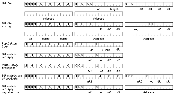
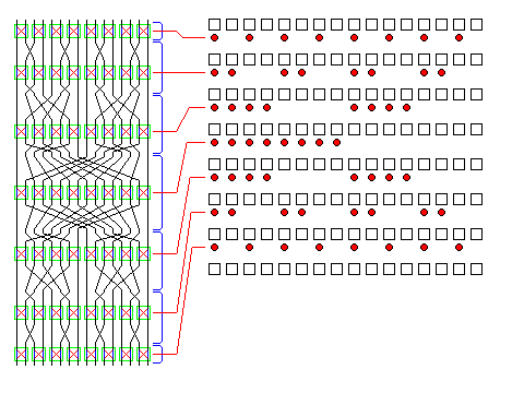
These are the formats of the extended operate instructions including the multi-stage transpose instructions:
These instructiona are all available from Normal Mode.
In Compact Mode, the instructions of the form 00xxxx and 01xxxx are available, but the ones for population count, bit matrix multiply, and multi-stage transpose are not available.
In Simple Mode, the instructions for population count, bit matrix multiply, and multi-stage transpose are also not available. Those instructions that are available have different opcodes as follows:
                                  Normal  Simple
                                  Compact
                                  ------  ------
Bit field                         010522  045220
Bit field string                  010544  045440
Bit matrix sum of products        001100  111000
Bit matrix multiply register load 001111  111110
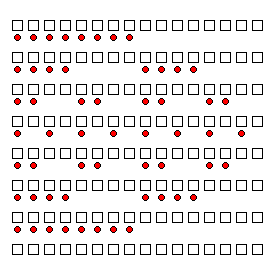
This diagram illustrates how the population count instruction, which is also capable of performing other functions, operates:
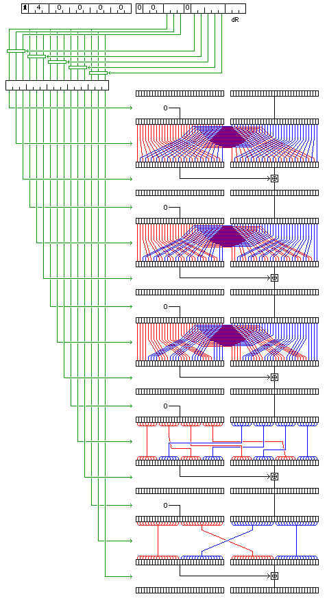
This instruction, the SEBI (Separate Bits) instruction, with the opcode 140000 00xxxn (note that this opcode corresponds to what would have been an unaligned load byte instruction, which, of course, is not required, as a normal load byte instruction has no alignment restriction), operates on arithmetic/index registers n and n+1, performing up to fifteen operations in sequence on the contents of those two registers, as indicated by the last nine bits of the instruction.
The instruction with opcode 140000 00737n of this type causes arithmetic/index register n+1 to contain a count of the number of 1 bits originally contained in both registers.
The instruction with opcode 140000 00634n of this type causes the eight bytes of registers n and n+1 to each contain an 0 or a 1 depending on whether the corresponding bit of the last byte of register n+1 was initially an 0 or a 1.
The instruction with opcode 140000 00234n of this type performs a matrix transpose on the 64 bits of those two registers, if they are thought of as being an 8 by 8 matrix of bits. Combining the 140000 00634n and 140000 00234n instructions with shift instructions permits the efficient manipulation of individual bits in a computer word.
Because the usefulness of the addition operation would be limited by unwanted carries if it is not accompanied by the preceding clear half operation, if the bit for the clear half operation is not set, the bit indicating the addition operation may be used to indicate a different operation instead.
This mode also provides for bit field operations, whose instructions have the opcodes
010522 1001xx  CBF    Compare Bit Field
010522 1002xx  MBF    Move Bit Field

010522 1004xx  ABF    Add Bit Field
010522 1005xx  SBF    Subtract Bit Field

010522 1010xx  NBF    AND Bit Field
010522 1011xx  OBF    OR Bit Field
010522 1012xx  XBF    XOR Bit Field
010522 1013xx  SWBF   Swap Bit Field
The six-bit length field of the instruction indicates the width of the field operated on in bits, minus one. The address field in the instruction and the index register contents, if indexing is used, are in units of bits, but the base register contents are still a byte address.
As with the regular memory-reference instructions in this mode, a zero base register value indicates that the 16-bit address field for the corresponding operand is replaced by a 32-bit field starting with a zero, and then containing 3-bit fields for each of the base register and the index register and a 25-bit address displacement.
The IBM 7030 computer, also known as the STRETCH, and the Univac III were computers that operated on bit fields of arbitrary length with bit addressing.
In addition, another form of bit field instruction is provided, also illustrated above allowing operations similar to the string operations to be performed on bit fields.
Here, the size of the bit fields is given by the dSize and sSize fields, and the length field gives the number of bit fields acted upon. The C bit indicates that the value in the arithmetic/index register cR is used (or that register and the register following it if sSize is greater than 32) to perform the following operation on the bit field values read from the source parameter: the bits in the positions of the input bit field corresponding to the 1 bits in the condensing register are placed in order in the least significant bit positions of the destination bit field.
Again, as with the regular memory-reference instructions in this mode, a zero base register value indicates that the 16-bit address field for the corresponding operand is replaced by a 32-bit field starting with a zero, and then containing 3-bit fields for each of the base register and the index register and a 25-bit address displacement.
The opcode used in this format is:
010544 000xxx xxxxxx 02xxxx MCBFS Move and Condense Bit Field String
This instruction is useful for translating between strings of bit fields and strings of bytes or other normally-aligned values which can then be efficiently operated on by other instructions.
Except for the fact that the condensed bits are placed in the least significant (rather than the most significant) portion of the result bit field, the condense operation which is repeatedly performed in this instruction is the same operation as is performed by the Pack instruction of the BESM-6 computer.
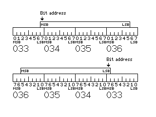
In normal operation, the bits of a byte are numbered from 0 to 7 from left to right. When the computer is operating in little-endian mode, with the bit indicating that the leftmost or most significant part of a quantity is in the portion with a higher address, the bits of a byte are numbered from 7 to 0 from left to right.
This permits bit addressing for these instructions to function in a consistent manner in both modes, as shown in the diagram below:
Another group of instructions belonging to this category are those associated with bit matrix multiply operations.
The bit matrix multiply instructions have the opcodes:
140000 02x1xx  BMM16    Bit Matrix Multiply 16
140000 02x2xx  BMM32    Bit Matrix Multiply 32
140000 02x3xx  BMM64    Bit Matrix Multiply 64
The bit matrix sum of products instructins have the opcodes:
001100 12x400 00x1xxx  BMSP16   Bit-Matrix Sum of Products 16
001100 12x400 00x2xxx  BMSP32   Bit-Matrix Sum of Products 32
001100 12x400 00x3xxx  BMSP64   Bit-Matrix Sum of Products 64
and the bit matrix multiply register load instructions have the opcodes:
001111 02x5xx  LBMM16  Load Bit-Matrix-Multiply 16
001111 02x6xx  LBMM32  Load Bit-Matrix-Multiply 32
001111 02x7xx  LBMM64  Load Bit-Matrix-Multiply 64
The multi-stage transpose instructions have the opcodes:
140000 02x5xx  MST16    Multi-Stage Transpose 16
140000 02x6xx  MST32    Multi-Stage Transpose 32
140000 02x7xx  MST64    Multi-Stage Transpose 64
The mR field in the instruction indicates one 256-bit short vector register for the BMM16 instruction. Originally, a group of four 256-bit short vector registers, with the values 0, 4, 8, and 12 indicating the first register of that group were the only ones allowed, for the BMM32 instruction, and that field was not used, and had necessarily been zero, in the BMM64 instruction.
However, as noted in the initial section of this page, implementations of this architecture may provide for register renaming to allow multiple threads to execute concurrently without context switching. Thus, it seemed reasonable to consider that a process might get more than its share of register space.
Even without taking such an extraordinary step, there is additional register space in the normal complement of registers that is only used in another mode, register scratchpad mode: thus, under normal circumstances, some additional values of the mR field in the BMM32 and BMM64 instructions are defined to make use of the supplementary floating-point registers. The table below shows how the mR field is interpreted normally, and when 4, 8, or 16 explicit bit-matrix-multiply register banks, each treated as containing 16 registers having the same size as a short vector register, have been allocated to a process:
    no allocation            4 allocated              8/16 allocated 8 allocated 16 allocated
    BMM16 BMM32    BMM64     BMM16 BMM32    BMM64     BMM16 BMM32    BMM64       BMM64

 0  SV 0  SV 0-3   SV 0-15   BM 0  BM 0-3   BM 0-15   BM 64 BM 0-3   BM 0-15     BM 0-15
 1  SV 1                     BM 1  BM 4-7             BM 65 BM 4-7               BM 16-31
 2  SV 2  SF 0-7             BM 2  BM 8-11  SV 0-15   BM 66 BM 8-11  BM 16-31    BM 32-47
 3  SV 3  SF 8-15            BM 3  BM 12-15           BM 67 BM 12-15 SV 0-15     BM 48-63
 4  SV 4  SV 4-7             BM 4  BM 16-19 BM 16-31  BM 68 BM 16-19 BM 32-47    BM 64-79
 5  SV 5                     BM 5  BM 20-23           BM 69 BM 20-23             BM 80-95
 6  SV 6  SF 16-23           BM 6  BM 24-27           BM 70 BM 24-27 BM 48-63    BM 96-111
 7  SV 7  SF 24-31           BM 7  BM 28-31           BM 71 BM 28-31             BM 112-127
 8  SV 8  SV 8-11  SF 0-31   BM 8  BM 32-35 BM 32-47  BM 72 BM 32-35 BM 64-79    BM 128-143
 9  SV 9                     BM 9  BM 36-39           BM 73 BM 36-39             BM 144-159
10  SV 10 SF 32-39           BM 10 BM 40-43 SF 0-31   BM 74 BM 40-43 BM 80-95    BM 160-175
11  SV 11 SF 40-47           BM 11 BM 44-47           BM 75 BM 44-47 SF 0-31     BM 176-191
12  SV 12 SV 12-15 SF 32-63  BM 12 BM 48-51 BM 48-63  BM 76 BM 48-51 BM 96-111   BM 192-207
13  SV 13                    BM 13 BM 52-55           BM 77 BM 52-55             BM 208-223
14  SV 14 SF 48-55           BM 14 BM 56-59 SF 32-63  BM 78 BM 56-59 BM 112-127  BM 224-239
15  SV 15 SF 56-63           BM 15 BM 60-63           BM 79 BM 60-63 SF 32-63    BM 240-255
These instructions perform a bit matrix multiply on values in the accumulator/index registers using the bits in the short vector register area to define the matrix. For the BMM16 instruction, the operands indicated by dR and sR are the least significant 16 bits of the registers they indicate; for the BMM32 instruction, they are the entire registers, and for the BMM64 instructions, they are pairs of registers, and the dR and sR fields, which indicate the first register of the pair, may only have the values 0, 2, 4, and 6. (This is not changed by the allocation of bit matrix multiply registers, of course.)
The logical operation performed to derive the output from the input, therefore, is that the source is ANDed to successive groups of 16, 32, or 64 bits in the bit-matrix-multiply register, and then all the bits in the 16, 32, or 64-bit long result are XORed together to form one bit in the final result.
These instructions allow the rapid application of matrix-based error-correcting codes, such as the Golay code, to data, and they also simplify some format conversion tasks.
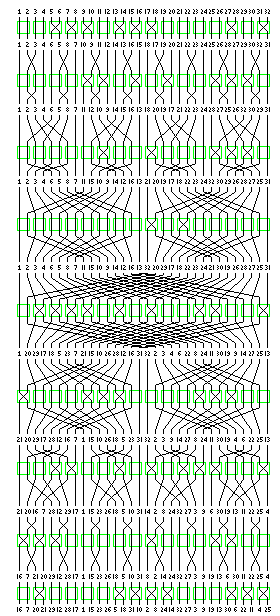
The Multi-Stage Transpose instructions are intended to allow rearrangements of bits without duplication to be specified using fewer registers than are required for a bit-matrix multiply. This is achieved through the use of a Beneš network, in the arrangement illustrated below for the MST16 and MST32 instructions:
This network, because it belongs to the class of networks known as rearrangeable networks, although it is not adequate for a telephone switchboard because it is not fully non-preemptive in the sense of always allowing a new connection to be made without disturbing existing connections, can be used to set up any possible permutation of its inputs.
Seven layers, each requiring an 8-bit input, suffice for the MST16 instruction; thus, only 56 bits are needed to specify such a transpose. Nine layers, each requiring a 16-bit input, are needed for the MST32 instruction, so, in this case, 144 bits are used, and this still fits easily in the 256 bits of a single short vector register. In the case of the MST64 instruction, as can be inferred from the pattern of the diagram above, eleven layers with a 32-bit input will be required, for a total of 352 bits each, and this will require a pair of short vector registers. Thus, the registers used to describe transpositions for this instruction (in each case, the bits used start with the leftmost bits of the first register specified) are:
    MST16 MST64
    MST32

 0  SV 0  SV 0-1
 1  SV 1
 2  SV 2  SV 2-3
 3  SV 3
 4  SV 4  SV 4-5
 5  SV 5
 6  SV 6  SV 6-7
 7  SV 7
 8  SV 8  SV 8-9
 9  SV 9
10  SV 10 SV 10-11
11  SV 11
12  SV 12 SV 12-13
13  SV 13
14  SV 14 SV 14-15
15  SV 15
It is not considered necessary to attempt to use the supplementary floating-point registers or to allocate bit-matrix-multiply registers for this instruction because of its reduced requirements.
The particular arrangement of the Beneš network shown above is chosen to make it understandable from the programmer's point of view, since in this arrangement, the operations performed by the individual stages can also be performed by AND, shift, and XOR instructions. As this diagram shows:
the stages in the network are chosen so that the bits controlling routing first switch a bit with the next bit, then switch bits in a group of two bits with the corresponding bits in the next group of two bits, and then switch bits in a group of four bits with the corresponding bits in the next group of four bits, and so on until the total number of bits to be rearranged is divided into halves, and then back again in reverse order.
I have since learned (in my web searches for more information describing the looping algorithm used to set up this type of network) that just such a type of instruction for a computer is the subject of U. S. Patent 6922472, granted on July 26, 2005; inventors Ruby B. Lee, Xiao Yang, and Manish Vachharajani; so apparently I have stumbled on a subject of active commercial research. It may also be noted that a related patent, U. S. Patent 6952478, deals with achieving the same end by means of an omega-flip network. A Beneš network is built from a butterfly network followed by an inverse butterfly network. On the page describing instructions for assisting with the Fast Fourier Transform, the structure of the classic Cooley-Tukey Fast Fourier Transform is exhibited, which corresponds to a butterfly network. The Pease framework, exhibited there, shows how an equivalent network can be achieved with the same structure for each stage. The omega-flip network uses that structure in its first half, and the inverse permutation in the second half, and so, instead of using AND, shift, and XOR, one can simply use one instruction to accomplish each stage of the transposition, that instruction belonging to one of two types, where the more elaborate hardware requirements of a full programmable Beneš network are not appropriate. |
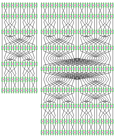
The arrangement shown in the diagram at right is also a Beneš network; it is formed from the arrangement shown above simply by rearranging the order of input and output bits. The rearrangement is that obtained by reversing the bits in the number of each bit position, when that number is represented in binary form.
In this arrangement, it is obvious that the two outer layers of the network are the only layers in which bits can be routed between the right and left halves, and that what lies within those layers is the next smaller Beneš network, repeated twice.
Given this, it is clear that it is necessary that the outer two layers must be able, for any permutation of outputs to inputs, to divide the bits (or signals, or flows) into two halves such that the same bits are in the same half of the network for further rearrangement by each of the two disjoint Beneš networks of lower order which lie within.
This is also a sufficient condition for a Beneš network of a given order to be able to perform any permutation if the Beneš network of the next lower order is able to perform any permutation. As the core network, a gate which can produce the permutations (1,2) or (2,1), provides all possible permutations of two elements, if the division into halves is possible at least for all pairs of layers with 4, 8, 16, 32, and so on switching elements, then by induction it is proven that the Beneš network does provide the ability to produce any possible permutation.
The algorithm for doing this was given in a paper in the Bell System Technical Journal by D. C. Opferman and N. T. Tsao Wu.
Since a given permutation will be split into halves correctly regardless of which half is the right half and which half is the left half, one can begin by choosing an arbitrary setting for one of the switches in one of the two layers.
This then implies which halves of the network within will be used for two of the signals. Set the two switches on the opposite outer layer that involve the two bits (or, of course, possibly just one switch) so as to route the two signals each to the right half. Then, the other two signals that have now been assigned to a definite half of the inner part of the network imply the settings of two switches in the original outer layer, or, possibly, just one.
Continue until just one switch is determined; this never results in a contradiction because as the area being assigned grows, the two new signals determined are always going to opposite halves. If not all signals are assigned, then begin with another arbitrary switch setting in the remaining area.
To illustrate this algorithm, using the arrangement for the Beneš network shown above, where we begin with odd and even as our two halves instead of left and right, here is how we would find the appropriate switch settings for Permutation P, from DES:
First, we establish the settings for the outermost layer:
 1  2  3  4  5  6  7  8  9 10 11 12 13 14 15 16 17 18 19 20 21 22 23 24 25 26 27 28 29 30 31 32
 1  2|     |     |     |     |     |     |     |     |     |     |     |     |     |     |
                   8  7                   16 15
       3  4
                        10  9                                           25 26
                                                                  23 24                   32 31
                                    14 13                                     28 27
                                                18 17 19 20
             6  5                                           21 22
                              11 12                                                 29 30


            29 12
                                                                               6 30 11 22

      21 20                         18  5
                  28 17                                                 19 13
                                                      14 24 32 27
                              23 26       10 31
                                                                   3  9                   25  4
16  7
     |     |     |     | 1 15|     |     |     | 8  2|     |     |     |     |     |     |
16  7 20 21 29 12 28 17  1 15 23 26  5 18 31 10  2  8 24 14 32 27  3  9 19 13 30  6 22 11  4 25
We arbitrarily set 1 and 2 on the top to be left alone; this puts 1 on the left of a pair, and 2 on the right of a pair. So on the other side, 1 and 15 are not swapped, but 2 and 8 are swapped. So now, 15 is on the right, 8 is on the left. Going back to the top, this determines that 7 and 8 are swapped, and so are 15 and 16. Now, 7 is on the right, 16 is on the left, and they happen to be in the same pair.
So now we start a new loop, arbitrarily choosing that 3 and 4 are not swapped. This establishes that 3 and 9 are not swapped on the bottom, and that 4 and 25 are swapped. And then this continues on, shown above proceeding from the outside in. This continues until 29 on the left and 12 on the right of the same pair are found, again in the output permutation, and at that point, nothing is left.
Then, we continue with the next inner layer, now divided into two permutations of 16 items.
The first permutation is:
 1  3| 6  8|10 11|14 16|18 19|21 23|25 28|29 32
 1  3
                              21 23       32 29
                  14 16             28 25
       6  8 11 10
                        18 19

                  18 10              6 19
                        14  8             11 25
21 16 28 29
             1 23             32  3
16 21|29 28| 1 23|18 10| 8 14|32  3|19  6|11 25
and the second permutation is:
 2  4| 5  7| 9 12|13 15|17 20|22 24|26 27|30 31
 2  4
                              22 24
       5  7
                        20 17             30 31
            12  9 15 13
                                    27 26

            15 26             27  9
      12 17                         30 13
20  7              5 31
                         2 24             22  4
 7 20|12 17|15 26| 5 31| 2 24|27  9|13 30|22  4
This then divides it into four permutations of eight items, each of which then becomes two permutations of four items:
 1  6|11 14|18 21|28 32      1 11|21 32      6 14|18 28
 1  6                        1 11            6 14
      11 14 21 18                 32 21           18 28
                  32 28
                             1 21 32 11     18 28
21 28       32 14           21  1|32 11            6 14
       1 18       11  6                     28 18|14  6
21 28| 1 18|14 32| 6 11
 3  8|10 16|19 23|25 29      3 10|19 29      8 16|23 25
 3  8                        3 10            8 16
      10 16                       29 19           23 25
            19 23 29 25
                            29 10  3 19     23 16  8 25
                  19 25     29 10| 3 19     16 23| 8 25
29 16 10 23
             3  8
16 29|23 10| 8  3|19 25
 2  5|12 15|20 22|27 30      2 15|20 30      5 12|22 27
 2  5                        2 15            5 12
      15 12       30 27           20 30           22 27
            20 22
                            20 15  2 30           22 27
20 12             30 22     20 15| 2 30      5 12
      15  5  2 27                           12  5|27 22
20 12|15  5| 2 27|30 22
 4  7| 9 13|17 24|26 31      4  9|17 26      7 13|24 31
 4  7                        4  9            7 13
       9 13 17 24                 17 26           24 31
                  26 31
                            17 26            7 31 24 13
      26 31                        4  9      7 31|24 13
             9 24           17 26| 9  4
17  7              4 13
 7 17|26 31|24  9|13  4
at which point, the permutations of two items in the innermost layer may be determined directly.
The network that results is depicted at right. Note that the number of crossings is visibly low in the two layers adjacent to the innermost layer, where groups of four connections are acted upon. This is not a consequence of peculiarities in the permutation P chosen to illustrate; instead, it's a consequence of the convention of always choosing to leave the first pair of items considered not interchanged; and that is why of those two layers, the upper one is particularly low in interchanges.
The third line of the diagram above shows the format of an instruction which specifies two bit-matrix-multiply registers for another logical operation. Here, an intermediate result is formed by taking groups of bits from the input, selecting them by performing an OR with the inverse of the contents of the first bit-matrix multiply register, and then performing an AND over all the bits of the result to form one bit in the intermediate result. Then, bits from the intermediate result are selected by performing an AND with groups of bits from the second bit-matrix multiply, but this time a bit in the final result is formed by a normal inclusive OR over the bits of the result of the AND.
The bit matrix multiply registers allocated to a process, when the default six-bit opcode translation scheme is chosen, can be loaded by the instructions shown in the third line of the diagram above, and in which the sX and sB fields operate in the same manner as in standard memory-reference instructions.
The mR field in this instruction indicates the destination bit matrix multiply register in the same manner as the mR field in the BMM16, BMM32, or BMM64 instruction respectively, and so this instruction may, depending on the number of explicit bit matrix multiply registers allocated, load data into the short vector registers or the supplementary floating-point registers.