At this point, I now feel ready to illustrate how computing with 36-bit and 60-bit floating-point numbers in the context of an architecture built around a 48-bit word and a 192-bit wide path to memory might look in more detail.
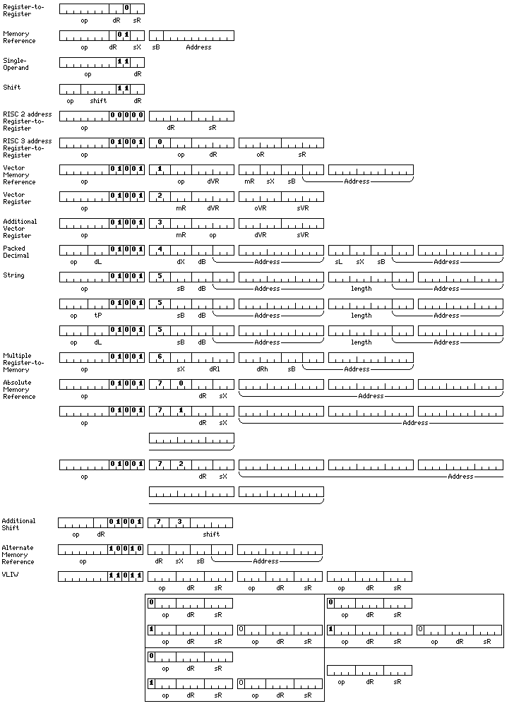
This diagram illustrates the addressing modes and instruction formats that I envision in this hypothetical architecture:
The standard convention that 0 in an index register field means that an instruction or an address within an instruction is not indexed is used.
The opcodes for register-to-register instructions would be as follows:
     0-   1-   2-   3-    4-   5-    6-   7-
  -0 SWF  SWD  SWM  SWE   SWH  IH    SW   I
  -1 CF   CD   CM   CE    CH   UCH   C    UC
  -2 LF   LD   LM   LE    LH   ULH   L    UL
  -3 STF  STD  STM  STE   STH  LH    ST   X
  -4 AF   AD   AM   AE    AH   NH    A    N
  -5 SF   SD   SM   SE    SH   OH    S    O
  -6 MF   MD   MM   ME    MH   MEH   M    ME
  -7 DF   DD   DM   DE    DH   DEH   D    DE
These opcodes would also be used for scratchpad-to-scratchpad instructions. and several other instruction types, including the memory reference instructions of the form
oo11rxbaaaaa
The alternate memory reference instructions, also of type RX, having the form
oo55rxbaaaaa
would, when indexed, have the following opcodes:
     0-     1-
  -0 SWFCX  SWDCX
  -1 CFCX   CDCX
  -2 LFCX   LDCX
  -3 STFCX  STDCX
  -4 AFCX   ADCX
  -5 SFCX   SDCX
  -6 MFCX   MDCX
  -7 DFCX   DDCX
The suffix CX stands for Converted Index, and indicates that the scheme of avoiding division by three or by five to pack three 60-bit floats or five 36-bit floats in a 192-bit memory word which will be more fully explaned on a later page is used, and thus if the instruction is indexed, the index is in units of 36 bits or 60 bits, with additional spacing for quick aligned retrieval, rather than in units of 12 bits, the normal fundamental unit of addressing.
In the case of 60-bit double-precision numbers, what happens is this:
Three such numbers can be packed in a single 192-bit memory line, leaving 12 bits of wasted space. Hence, 32 such numbers can be placed in 11 memory lines, wasting space for one 60-bit number in addition to 12 bits in each memory line; the advantage of this is that the time-consuming operation of division (even by three) is avoided.
In the case of 36-bit single-precision numbers:
Five such numbers can be packed in a single 192-bit memory line, leaving 12 bits of wasted space. Hence, 64 such numbers can be placed in 13 memory lines, wasting space for one 36-bit number in addition to 12 bits in each memory line; the advantage of this is that the time-consuming operation of division (even by five) is avoided.
The diagram below illustrates how arrays of 36-bit and 60-bit floating-point numbers would be stored in this computer with the assistance of CX type instructions; the conventional storage of 48-bit floating-point numbers is also shown for comparison.
The fourth item in this image shows an alternative technique available when arrays containing an equal number of elements for both single and double precision numbers are available; the elements can be interlaced, and treated as if they are 96 bits long with conventional indexing techniques, not using CX instructions. (It is primarily because this option is available that double precision is not simply 64 bits long, which would also fit three to a 192-bit memory word, and without 12 bits left over. This is notwithstanding the notes on design rationale given above, since after the choice of 36-bit and 60-bit floats led to an architecture built around a 48-bit word, and then the measures required to access those sizes of floats without leading to multiple fetches for unaligned operands, or excessive waste of memory space, led to a 192-bit wide memory bus, the fact that 64-bit floats would fit, plus the pressures of compatibility with a world of computing built around the 8-bit byte, still strongly suggest reconsideration.)
It is expected that compilers (well, at least, FORTRAN compilers) for this architecture will take advantage both of the converted index method of storing arrays, and of the possibility of interleaving single precision and double precision arrays, wherever possible and appropriate.
This is a comparison of how storage of 60-bit and 64-bit values in 192-bit memory words, using the Converted Index techique, would appear:
An alternate mode of operation, in which double precision floats are 64 bits in length, is not out of the question for this architecture. However, accessing memory in this way facilitates something perhaps more useful: an alternate mode of operation in which a computer based on the 8-bit byte and having a 64-bit path to memory is emulated, thus potentially even allowing a chip implementing the architecture described here to also have access to pre-existing software.
If, instead, only data-type interoperability is sought, and a custom architecture such as the one described here is used, those features which depend on a 256-bit path to memory should be omitted.
When not indexed, these opcodes would instead be used for the jump instructions:
     0-     1-
  -0 JMS    JV
  -1 JL     IXJL
  -2 JE     JC
  -3 JLE    IXJLE
  -4 JH     DXJH
  -5 JNE    JNC
  -6 JHE    DXJHE
  -7 JNV    JMP
The auxilliary memory-reference instructions, which are longer, will permit fully indexed jump instructions, as well as operations on other datatypes; it is necessary to use only a limited number of instructions in the alternate memory-reference instruction format because 32-bit instructions of the form
oo55xxxxxxxx
are also needed for multiple register to memory instructions (format RMS), scratchpad shift instructions (format ASH), and vector register instructions (format VV).
The various basic operations are:
Integer and Floating:
 SW   Swap
 C    Compare
 L    Load
 ST   Store
 A    Add
 S    Subtract
 M    Multiply
 D    Divide

Integer only:
 I    Insert
 UC   Unsigned Compare
 UL   Unsigned Load
 X    Exclusive OR
 N    And
 O    OR
 ME   Multiply Extensibly
 DE   Divide Extensibly

Floating only:
 MEU  Multiply Extensibly Unnormalized
 DEU  Divide Extensibly Unnormalized
 LU   Load Unnormalized
 STU  Store Unnormalized
 AU   Add Unnormalized
 SU   Subtract Unnormalized
 MU   Multiply Unnormalized
 DU   Divide Unnormalized
The various data types, indicated by suffixes, are:
Q    Quarter-word 12-bit fixed point
H    Halfword     24-bit fixed point
(no suffix)       48-bit fixed point
L    Long         96-bit fixed point
F    Floating     36-bit floating point
D    Double       60-bit floating point
M    Medium       48-bit floating point
E    Extended     96-bit floating point
The jump instructions are:
JMS   Jump to Subroutine
JL    Jump if Low
JE    Jump if Equal
JLE   Jump if Low or Equal
JH    Jump if High
JNE   Jump if Not Equal
JHE   Jump if High or Equal
JNV   Jump if No Overflow
JV    Jump if Overflow
IXJL  Increment Index and Jump if Low
JC    Jump if Carry
IXJLE Increment Index and Jump if Low or Equal
DXJH  Decrement Index and Jump if High
JNC   Jump if No Carry
DXJHE Decrement Index and Jump if High or Equal
JMP   Jump
The JMS instruction uses the index register field to indicate in which of the base registers the return address of the instruction is to be stored. In this case, zero may be used as a valid value, leading to the return address being stored in base register zero, the one that is not used as a register containing a base address.
In the case of the IXJL, IXJLE, DXJH, and DXJHE instructions, the index field indicates an arithmetic register used as a loop counter, and the target address of the jump, to be taken as long as the loop remains in progress, is not indexed.
Note that only the Extended precision floating point numbers can be unnormalized, since the others have a hidden first bit: the floating-point formats used are as shown below:
Floating-point and integer data is stored in big-endian format; that is, the most significant or leftmost portion of a data item is stored in the 12-bit memory cell having the lowest address.
It might be worthwhile to briefly explain the basic rationale behind this design here:
The 36-bit format was introduced, despite the lengths required to accomodate it, because its mantissa field matches that of the IBM 7090, and it was felt by many programmers at the time of the introduction of the IBM System/360 that the precision that earlier computer offered allowed single precision to be useful in many more circumstances. The additional bit present due to the hidden first bit was given to the exponent, so that the exponent range could be similar to the larger range offered by the IBM System/360.
The 60-bit format was then added because a double-precision format was needed, but as even 64 bits offered a level of precision excessive for almost any purpose, instead of going to the natural 72-bit mate for 36-bit single precision, the same size of double-precision float as used on the Control Data 6600 computer, renowned for its usefulness in scientific computation, was used.
Given 36-bit and 60-bit floating-point formats, their common unit is 12 bits in length. Thus, for normal operations, data types should be a power of two multiple of 12 bits in length. This suggested a 48-bit floating-point type; such a type, having a precision just over ten decimal digits, corresponds to the precision of most pocket calculators, and thus suggested itself as possibly being the most useful general-purpose floating-point format, in addition to being the simplest one to use on this architecture.
And thus 96 bits was the most natural length, given that other architectures have used 80 and 128 bits, for extended precision numbers to round out an attempt to adapt the IEEE 754 standard to octal hardware.
The architecture includes eight 48-bit long fixed-point registers and eight 96-bit long floating-point registers as well as eight 48-bit long base registers; there are also 64 supplementary fixed-point registers; these are 96 bits long, which is why there is an opcode for an Insert instruction, to load the least significant 48 bits of a supplementary fixed-point register without altering the most significant 48 bits of that register; and 64 supplementary floating-point registers, which are 96 bits long like the ordinary registers. This also applies to the Unsigned Load instruction, which always clears the more significant bits, unlike the Load instruction, which performs sign extension.
The branch instructions are:
BRS   Branch to Subroutine
BL    Branch if Low
BE    Branch if Equal
BLE   Branch if Low or Equal
BH    Branch if High
BNE   Branch if Not Equal
BHE   Branch if High or Equal
BNV   Branch if No Overflow
BV    Branch if Overflow
IXBL  Increment Index and Branch if Low
JC    Branch if Carry
IXBLE Increment Index and Branch if Low or Equal
DXBH  Decrement Index and Branch if High
BNC   Branch if No Carry
DXBHE Decrement Index and Branch if High or Equal
BRA   Branch
The looping instructions (IXBL, IXBLE, DXBH, and DXBHE) use the index field to indicate an arithmetic register, while the BRS instruction uses the index field to indicate a base register; in the other branch instructions, the index field is unused and should contain zero. Note that the BRS instruction can also be used to load a base register with an initial value, to permit addresses within a program it begins to be accessed by base-relative addressing.
It would not be necessary to omit explicit indication of parallelism, although it works by including a block of 16 or 32 bits at the beginning of each 256 bits of instructions, since instructions are fetched serially. Given that a similar feature is an inherent part of the parent architecture, and is not optional, presumably it would be required for efficient operation in the alternate architecture as well; however, multithreading would allow some threads which do not facilitate being as efficiently pipelined as others to execute without consuming a disproportionate share of resources, even if they take more elapsed time to accomplish equivalent processing, so emulation of architectures without an explicit indication of parallelism feature is not excluded.
It might even be possible to retain the short vector instructions, since, after all, current computer architectures that are implemented with a 64-bit path to memory also include similar features, often with block sizes of 128 or even 256 bits.
However, the various data memory width control features, tempting as it might be to retain them for fuller interoperability with the parent architecture, would be very inefficient without the 256-bit data path around which they were designed.
One important practical consideration is that present-day memory modules support loads and stores of individual eight-bit fields within a 64-bit memory word, but this architecture would instead benefit from the ability to load and store individual twelve-bit fields. Of course, writing a whole word with the appropriate part changed remains an option. Also, if 64-bit emulation is also present, both modes are useful, which suggests memory with the ability to handle individual four-bit fields would be preferred. Also note that eight ECC bits are only required for every 96 bits of data instead of every 64 bits, as the fundamental limit is 120 bits.
Thus, in a CX type instruction, the contents of the index register are converted to a displacement in units of 12 bits as follows:
For 60-bit floating-point numbers:
The part excluding the last five bits is multiplied by 176 (multiplied by 11 and shifted left by four bits) to indicate which 192-bit memory line is to be fetched;
Through a table lookup, the last five bits in effect are divided by three, with the quotient multiplied by 16 (to be the address of which of the 11 memory lines in a block is to be used), and the remainder, which may be 0, 1, or 2, multiplied by five (the length in units of 12 bits of a 60-bit floating-point number);
The three results obtained in this way are added to form the converted address.
For 36-bit floating-point numbers:
The part excluding the last six bits is multiplied by 208 (multiplied by 13 and shifted left by four bits) to indicate which 192-bit memory line is to be fetched;
Through a table lookup, the last six bits in effect are divided by five, with the quotient multiplied by 16 (to be the address of which of the 13 memory lines in a block is to be used), and the remainder, which may be 0, 1, 2, 3, or 4, multiplied by three (the length in units of 12 bits of a 36-bit floating-point number);
The three results obtained in this way are added to form the converted address.
Shift operations:
   0-    1-    2-    3-    4-    5- 6- 7-
-0 SHLH  SHL   SHLQ  -     SHLL  -  -  -
-1 SHRH  SHR   SHRQ  -     SHRL  -  -  -
-2 -     -     -     -     -     -  -  -
-3 ASRH  ASR   ASRQ  -     ASRL  -  -  -
-4 ROLH  ROL   ROLQ  -     ROLL  -  -  -
-5 RORH  ROR   RORQ  -     RORL  -  -  -
-6 RLCH  RLC   RLCQ  -     RLCL  -  -  -
-7 RRCH  RRC   RRCQ  -     RRCL  -  -  -
the shift operations being:
SHL  Shift Left
SHR  Shift Right
ASR  Arithmetic Shift Right
ROL  Rotate Left
ROR  Rotate Right
RLC  Rotate Left through Carry
RRC  Rotate Right through Carry
with the type suffixes as for the memory-reference instructions.
Packed Decimal and String Instructions:
   0-    1-    2-    3-    4-     5- 6- 7-
-0 -     -     -     -     MESTP  -  -  -
-1 CC    CB    CQ    CU    CP     -  -  -
-2 MVC   MVB   MVQ   MVU   MVP    -  -  -
-3 -     -     -     -     DSTRP  -  -  -
-4 TC    TB    TQ    TU    AP     -  -  -
-5 -     -     -     -     SP     -  -  -
-6 FMTC  FMTB  FMTQ  FMTU  MP     -  -  -
-7 SCC   SCB   SCQ   SCU   DP     -  -  -
The string and packed decimal operations are:
C     Compare
MV    Move
T     Translate
FMT   Format
SC    Scan

MESTP Multiply Extensibly and Store Packed
CP    Compare Packed
MVP   Move Packed
DSTRP Divide and Store Remainder Packed
AP    Add Packed
SP    Subtract Packed
MP    Move Packed
DP    Divide Packed
and the type suffixes, used with the string instructions to indicate the type of character operated on, are:
C Character     6-bit
B Byte          8-bit
Q Quarterword  12-bit
U Unicode      16-bit
Note that the operands of string instructions, unlike those of packed decimal instructions, cannot be indexed. The field marked tP indicates the register containing a pointer to the translate table used for translate instructions. Translate, Format, and Scan are translate instructions. For other string instructions, an index register field for the sourse operand, marked sX, occupies the same bit positions.
The operations performed by the various string instructions are described here.
MESTP replaces the source operand by the most significant part of the product, and DSTRP replaces the source operand by the remainder of the division, in addition to placing the normal result of packed multiplication or division respectively in the destination operand.
The nine-bit length field in a string instruction indicates the length of the string operand in individual characters, whatever the size of a character. Operands should be aligned on 24-bit boundaries if the character is 8 bits in length, and on 48-bit boundaries if the character is 16 bits in length.
The three-bit length fields in packed decimal instructions indicate the length of each operand in units of 12 bits, each containing three digits.
While this description of an architecture is now somewhat fleshed out, it still omits many details. The field marked stR in vector instructions indicates a register containing the stride, if zero, the stride is 1; that is, there is no stride. Instructions needed for converting between binary and packed decimal, and for packing and unpacking, are not given, nor are instructions for returning from interrupts, making a supervisor call, or loading and storing the program status word - or even switching between Scientific and General mode, which determines whether extra fixed-point or extra floating-point data types are made available in standard memory-reference and register-to-register instructions.
For many types of instruction, unlike the standard memory-reference instructions, more than 64 opcodes were not needed. For them, the supplementary bit should be zero, as it may be used later for future expansion.
But it should illustrate that a computer which handles floating-point data items of commensurate but not strict power-of-two lengths is possible without compromising efficient addressing and memory access. A floating-point ALU that is built to handle items of the length required, and not more, will have lower latency, and given the high demands of advanced scientific computing, an architectural contribution even of limited benefit is worth considering.
While the opcode is shown as six bits in length, it actually would be preferable if it were seven bits in length. Fortunately, this can be used to solve another problem: with an architecture based on units of 12 bits instead of 16 bits, fetching a 192-bit instruction bundle from memory would seem to require wasted space if the first 16 bits were used to indicate, for rapid instruction decoding, which of the 16 12-bit units in the 192-bit instruction bundle were the beginning of an instruction.
Thus, the first 24 bits of a 192-bit instruction bundle might not contain any portions of instructions. Instead, they are divided into three 8-bit bytes. A byte may contain any of 256 possible values. This exceeds the 243 possible values of five ternary digits.
Thus, we have fifteen ternary digits. The first fourteen of them refer to the fourteen 12-bit units which remain in the 192-bit instruction bundle. The fifteenth refers to the first 12-bit unit used for instructions (which will be the third 12-bit unit) in the following instruction bundle. That provides the information needed to determine whether the last instruction in the current bundle can be decoded immediately, or if it must be held over until the next bundle is fetched.
The ternary digits have the following meanings:
0 Not the beginning of an instruction
1 The beginning of an instruction; insert supplementary bit with value 0
2 The beginning of an instruction; insert supplementary bit with value 1
The supplementary bit can be considered to be inserted between the first three and the last three bits of the six-bit opcode.
Note that the fifteenth ternary digit is used solely to indicate whether the final instruction in a block terminates at the end of the block, and it is not necessary, in the case that the instruction does so terminate, that this ternary digit shall correctly indicate the supplementary bit value for the first instruction of the next block, if there is a subsequent block of instructions. (Of course, there need not be, since every program must come to an end somewhere.)
This raises a question, however. What if it's also desirable to explicitly indicate if an instruction can execute independently of the previous instructions in the block, or if there is a dependency issue? Wouldn't that require adding 16 bits for that purpose, again leaving an 8-bit hole in the instruction block?
Perhaps not. After all, this information is only required for instructions, not 12-bit memory cells that don't begin an instruction. So, one could use base-5 digits:
0 Not the beginning of an instruction
1 Independent, supplementary bit 0
2 Independent, supplementary bit 1
3 Dependent, supplementary bit 0
4 Dependent, supplementary bit 1
Five to the third power is 125, so three quinary digits can be stored in seven bits. Fifteen such digits, therefore, take up 35 bits, one bit less than 36 bits, so the number of bits required is increased by 11, and thus the efficiency of coding this information as well with each block of instructions is acceptable.
The original version of this architecture presented here required the use of the supplementary bit, and the opcodes were as follows:
Scientific Mode
 Supplementary Bit = 0
     0-   1-   2-   3-     4-   5-     6-   7-
  -0 SWH  SW   SWF  SWFCX  SWD  SWDCX  SWM  SWE
  -1 CH   C    CF   CFCX   CD   CDCX   CM   CE
  -2 LH   L    LF   LFCX   LD   LDCX   LM   LE
  -3 STH  ST   STF  STFCX  STD  STDCX  STM  STE
  -4 AH   A    AF   AFCX   AD   ADCX   AM   AE
  -5 SH   S    SF   SFCX   SD   SDCX   SM   SE
  -6 MH   M    MF   MFCX   MD   MDCX   MM   ME
  -7 DH   D    DF   DFCX   DD   DDCX   DM   DE

 Supplementary Bit = 1
  -0 IH   I    -    JMS    -    JV     -    MEUE
  -1 UCH  UC   -    JL     -    IXJL   -    DEUE
  -2 ULH  UL   -    JE     -    JC     -    LUE
  -3 XH   X    -    JLE    -    IXJLE  -    STUE
  -4 NH   N    -    JH     -    DXJH   -    AUE
  -5 OH   O    -    JNE    -    JNC    -    SUE
  -6 MEH  ME   -    JHE    -    DXJHE  -    MUE
  -7 DEH  DE   -    JNV    -    JMP    -    DUE

General Mode
 Supplementary Bit = 0
  -0 SWH  SW   SWQ  -      SWL  -      SWM  SWE
  -1 CH   C    CQ   -      CL   -      CM   CE
  -2 LH   L    LQ   -      LL   -      LM   LE
  -3 STH  ST   STQ  -      STL  -      STM  STE
  -4 AH   A    AQ   -      AL   -      AM   AE
  -5 SH   S    SQ   -      SL   -      SM   SE
  -6 MH   M    MQ   -      ML   -      MM   ME
  -7 DH   D    DQ   -      DL   -      DM   DE

 Supplementary Bit = 1
  -0 IH   I    IQ   JMS    -    JV     -    MEUE
  -1 UCH  UC   UCQ  JL     UCL  IXJL   -    DEUE
  -2 ULH  UL   ULQ  JE     ULL  JC     -    LUE
  -3 XH   X    XQ   JLE    XL   IXJLE  -    STUE
  -4 NH   N    NQ   JH     NL   DXJH   -    AUE
  -5 OH   O    OQ   JNE    OL   JNC    -    SUE
  -6 MEH  ME   MEQ  JHE    MEL  DXJHE  -    MUE
  -7 DEH  DE   DEQ  JNV    DEL  JMP    -    DUE
Note how 3 and 5, as the first digit of an opcode, because they were used for the converted index instructions, were available for different instructions, the jump instructions, when indexing was not in use.
To make it completely unnecessary to use the supplementary bit, further instruction formats have been introduced on this principle; thus, there are longer format instructions for additional register to register instructions, additional scratchpad to scratchpad instructions, and additional memory-reference instructions. In addition, there is some opcode space for a few alternate memory-reference instructions which are not increased in length; it is intended that this serve for the jump instructions.
In that case, the prefix area in a 192-bit instruction bundle would not be needed, but if explicit indication of parallelism is desired, ternary digits only would be required, with the meanings:
0 Not the first part of an instruction
1 Independent
2 Dependent
An alternative method of operating without a supplementary bit increases, rather than decreasing, the data types available.
If one excludes the 12-bit register to register instruction format, then the opcode field can be expanded to nine bits, with only the following three bits indicating the instruction mode.
Register to register instructions could be 24 bits long, having the following form:
 -----------------------------------------------
|        op       |  4  |  op |  dR |  op |  sR |
|     |     |     |     |     |     |     |     |
| | | | | | | | | | | | | | | | | | | | | | | | |
 -----------------------------------------------
 0     3     6     9    12    15    18    21
since shift instructions, like the packed decimal and string instructions, only require a six-bit opcode; bits 6 through 8 of those instructions would be zero. Note that here, unlike the case with register/scratchpad instructions, it is the last three bits of the opcode, not the first three bits, which are moved to bit positions 12 through 14.
One of the additional data types made possible by this would be 60-bit Chen-Ho encoded fixed-length packed decimal numbers. They would be eighteen digits long, with a range from -500,000,000,000,000,000 to +499,999,999,999,999,999 through the use of ten's complement notation for negative numbers.
So that the values 3 and 5 would appear in the same location within an instruction, to facilitate distinguishing the scratchpad to register and register to scratchpad instructions, a nine-bit opcode would be in the form aaabbbpps where the "logical" order of the bits in the opcode would be ppaaasbbb, ppaaa indicating the type, sbbb indicating the operation.
Further thought has led me to consider another shape that an instruction set architecture based on a 12 bit unit might take:
The first four lines show a very simple CISC instruction set.
Seven bits are allocated to the opcode, which means that there is no difficulty handling the data types to be used; 12, 24, and 48 bit integers, each with 16 basic operations; 36, 48, and 60 bit normalized floating-point numbers, each with 8 basic operations; and 96 bit extended precision floating point numbers, without a hidden first bit, with 16 basic operations. A few opcodes are left to allow conditional jump, subroutine jump, and load address instructions, for example.
Only one bit indicates the address mode for the source operand, and there are only four registers available in these modes for each data type. Furthermore, only two registers are allowed to be the destinations of memory-reference instructions, in order to allow single-operand instructions and shift instructions to be present within this basic set of instructions.
The usual values of the seven-bit opcodes are:
     00-  01-    02-  03-    04-  05-    06-  07-
  -0 JMS  JV     SWH  IH     SW   I      SWL
  -1 JL   IXJL   CH   UCH    C    UC     CL   UCL
  -2 JE   JC     LH   ULH    L    UL     LL
  -3 JLE  IXJLE  STH  XH     ST   X      STL  XL
  -4 JH   DXJH   AH   NH     A    N      AL   NL
  -5 JNE  JNC    SH   OH     S    O      SL   OL
  -6 JHE  DXJHE  MH   MEH    M    MEX    ML   MEL
  -7 JNV  JMP    DH   DEH    D    DEX    DL   DEL

     10-  11-    12-  13-    14-  15-    16-  17-
  -0 SWF  SWFCX  SWM  CVB    SWD  SWDCX  SWE  MEUE
  -1 CF   CFCX   CM   CVD    CD   CDCX   CE   DEUE
  -2 LF   LFCX   LM   LB     LD   LDCX   LE   LUE
  -3 STF  STFCX  STM  STB    STD  STDCX  STE  STUE
  -4 AF   AFCX   AM   LBA    AD   ADCX   AE   AUE
  -5 SF   SFCX   SM          SD   SDCX   SE   SUE
  -6 MF   MFCX   MM   LA     MD   MDCX   ME   MUE
  -7 DF   DFCX   DM   NMI    DD   DDCX   DE   DUE
The Multiply Extensibly instructions place the double-width product of the source operand and the destination operand in the register specified by the destination operand, treated as having twice the width as that implied by the name of the instruction. In the case of Multiply Extensibly Long (MEL), the destination operand is a register pair, it must be an even-numbered register, and the multiplicand is taken from the register following the one indicated by the instruction.
The Divide Extensibly instructions have a double-width destination operand; this is divided by the source operand, with the quotient left in the destination register (or, in the case of Divide Extensibly Long, DEL, in the destination register pair) and the remainder, a single-width quantity, is placed in the register preceding.
LBA is Load Base (Register) with Address, LA is Load Address; both load the target register with their effective addresses. LB and STB load and store values in base registers.
The jump instructions, which are of the forms 00x and 01x, as well as the converted index instructions, of the forms 11x and 15x, are, of course, not applicable to register-to-register instructions, only to memory-reference instructions. Also, those register-to-register instruction formats that are symmetrical in the sense of having the same set of registers specified as the destination and the source register do not include any of the store instructions, only the load instructions.
The NMI (Normalize) instruction is only available as a register to register instruction. It shifts the source register left until its first bit is 1, and it increments the destination register by 1 for each shift, if any, thus performed.
The CVD (Convert to Decimal) and CVB (Convert to Binary) instructions are applicable only to those memory-reference instruction formats in which the index register field is at least three bits long.
These instructions cannot be indexed. The index register field instead contains the length, in 12-bit halfwords, of the destination operand in memory, which is a packed decimal quantity. The Convert to Binary instruction converts that quantity to binary, storing it in the destination register; the Convert to Decimal instruction stores the value in the destination register, converted to packed decimal, in the source operand in memory.
The shift instructions, shown in the fourth line, have the opcodes:
000 SHL  Shift Left
001 SHR  Shift Right

011 ASR  Arithmetic Shift Right
100 ROL  Rotate Left
101 ROR  Rotate Right
110 RLC  Rotate Left through Carry
111 RRC  Rotate Right through Carry
and they have the limitation that only shift instructions that treat the four registers as 24-bit registers are available, not ones operating on 12-bit or 48-bit registers in this instruction format.
The single-operand instructions, shown in the third line, are:
0 100 000 CLR Clear
0 100 001 INV Invert
0 100 010 INC Increment
0 100 011 TCM Two's Complement

0 101 000 LBP Load Base with Program Counter

0 101 010 LP  Load from Program Counter
0 101 011 RTS Return from Subroutine
LBP loads a base register with the current program counter value; LP loads a normal integer register (which can be used either for arithmetic or as an index register) with the current program counter value. RTS loads the program counter from the register specified.
The fifth and sixth lines show a standard and an extended RISC instruction set. Here, there are two sets of 64 registers; one set consists of 48-bit integer registers, the other consists of 96-bit floating-point registers.
In the fifth line, we have only the basic operations available in other modes, and the instructions are two-address instructions. In the sixth line, the instructions are three-address ones instead, and there are three additional opcode bits. Also, three zero bits indicate the mode; they can have other values for future expansion of the instruction set; for example, vector instructions aren't shown here.
The next few lines illustrate additional instructions which provide the capabilities of large CISC machines; vector instructions on the one hand, and packed decimal and string instructions on the other. The twelfth line shows the format of character translation instructions, and the thirteenth that of instructions which convert between packed decimal and string.
The opcodes of the packed decimal instructions are:
0010 MVP Move Packed

0100 AP  Add Packed
0101 SP  Subtract Packed
0110 MP  Multiply Packed
0111 DP  Divide Packed

1111 DPR Divide Packed with Remainder
The Divide Packed instruction operates like other divide instructions, dividing the destination by the source, and leaving the quotient in the destination. The Divide Packed with Remainder instruction divides the destination by the source, leaving the remainder in the destination, and the quotient in the source.
The string instructions with four-bit opcodes are:
0010 T  Translate

0100 P  Pack
0101 U  Unpack
They assume 12-bit characters, and the Unpack instruction creates ASCII characters padded on the left with zeroes; that is, the four-bit quantity placed in the least significant part of each 12-bit character is preceded by 0000 0011.
The string instructions with seven-bit opcodes are:
1000010 MVH Move Halfwords
Also, the fourteenth line shows the format of instructions that save and restore multiple registers at once, useful for context switching.
These instructions have the opcodes:
0 110 010 LM   Load Multiple
0 110 011 STM  Store Multiple

1 110 010 LMF  Load Multiple Floating
1 110 011 STMF Store Multiple Floating
The load and store multiple instructions load and store 48-bit fixed-point registers, and the load and store multiple floating instructions load and store 96-bit floating-point registers, in their entirety, despite not being named long or extended instructions.
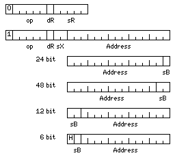
The fifteenth, sixteenth, and seventeenth lines (what I refer to as the sixteenth and seventeenth lines each take up two lines, with part of the instruction format indented) show the absolute indexed memory-reference format.
For the other formats of memory-reference instructions, if the base register field contains a zero, instead of following the System/360, and treating the address as absolute, array mode is used. In array mode, the contents of base register zero are added to the displacement to form an indirect address; the address in the location this points to then may have the contents of an index register added to it to form the effective address, if indexing is specified.
This avoids the problem that when arrays are larger than the range of displacements in an instruction, then a base register has to be used up just to access a single array. However, it has the limitation that, since it involves indirect addressing, an extra memory access is required whenever referencing an array.
The absolute indexed memory-reference format avoids this difficulty as well, since here no base register is required, as the displacement field is fully long enough to be a complete memory address in itself. Three forms of this format are provided, so as to avoid the need of putting the computer into different, incompatible, modes of operation; depending on the size of the memory available, a virtual address may be 36, 48, or 60 bits in length.
The eighteenth line provides additional shift instructions for 12 and 48 bit operands. These instructions have only four destination registers, and can be thought of as belonging to the simple CISC instruction set along with the instructions of the formats shown in the first four lines.
Their opcodes are:
01000 SHLH  Shift Left Halfword
01001 SHRH  Shift Right Halfword

01011 ASRH  Arithmetic Shift Right Halfword
01100 ROLH  Rotate Left Halfword
01101 RORH  Rotate Right Halfword
01110 RLCH  Rotate Left through Carry Halfword
01111 RRCH  Rotate Right through Carry Halfword

11000 SHLL  Shift Left Long
11001 SHRL  Shift Right Long

11011 ASRL  Arithmetic Shift Right Long
11100 ROLL  Rotate Left Long
11101 RORL  Rotate Right Long
11110 RLCL  Rotate Left through Carry Long
11111 RRCL  Rotate Right through Carry Long
In the nineteenth line, we have an expanded version of the memory-reference instruction that allows more registers to be used, and which provides a larger displacement. So in this line, we're back to CISC.
In the nineteenth line, we have instructions of the VLIW type. The seven bits that were usually used for the opcode instead indicate which data types will be acted on in the VLIW bundle; a 1 bit indicates an instruction referring to that data type will be present. The data types are, in order, 12, 24, and 48 bit integer, 36, 48, 60, and 96 bit floating-point.
Each of those data types corresponds to one 12 bit unit in the instruction, which may be present or absent - except in the case of the three floating-point sizes with a hidden first bit. Since the unnormalized floating-point instructions are not applicable to them, the opcode field is one bit shorter; only three bits long.
The extra bit can be 0 or 1; if it is 1, this indicates that there will be two instructions for that data type in the current VLIW bundle. Only one of those instructions can be an add or subtract, and only one of them can be a multiply or divide. Also, the same register cannot be used twice for any purpose in the two instructions.
Since the adder and the multiplier are necessarily separate, while making the ALUs for each precision separate is a design decision made here for optimization, this extra complication seemed badly needed.
Optionally, allowing a multiply and a divide, and allowing up to three instructions for a type, may be possible as well.
12 bit integers use, of the 64 fixed-point registers, registers 16 through 31; 24 bit integers use registers 32 through 47, and 48 bit integers use registers 48 through 63.
The 64 floating-point registers are also divided into four parts, 0 to 15 for 36 bit floats, 16 to 31 for 48 bit floats, 32 to 47 for 60 bit floats, and 48 to 63 for 96 bit floats.
Because all the instructions in a VLIW bundle are using disjoint sets of registers, and they're using ALUs either of a different type or different precision, it is intended that all the instructions in such a bundle can be executed simultaneously.
Note also that VLIW instructions do not affect the condition codes since it isn't clear which of the instructions in a bundle one would want to have reflected in the condition codes. This is one reason for sometimes using other types of instruction (along with being able to access memory).
The extended memory-reference instructions use as their destination registers the first half of each group of 16 registers associated with each type. (Since all the registers are really the same length, that of the longest type for either integer or floating-point, all the RISC instructions can use all 64 registers.) For index registers, the first half of the 16 fixed-point registers used (in the VLIW format) for 48-bit integers are used. For base registers, fixed-point registers 8 through 15 are used.
In the instruction formats for the basic CISC set, in the first two lines, the first four registers of each group of 16 registers are used; for index registers, the first four of the fixed-point registers used for 48-bit integers in the VLIW format are used. For base registers, fixed-point registers 4 through 7 are used, since they point to regions of different size than the base registers used in the extended memory-reference instructions, different registers are used.
Since this ISA uses full seven-bit opcode fields, there is no need for a supplementary bit. Hence, a full-VLIW mode cannot be made to fit more effectively into a 12-bit unit by using ternary or quinary digits in the way that was used for the previous ISA on this page.
However, I have thought of another way to make a virtue of a necessity.
In VLIW mode, the instruction stream will be divided into 96-bit blocks, each containing eight 12-bit units.
The first unit will be divided into six two-bit parts, interpreted as follows:
00 - Not the beginning of an instruction
01 - The beginning of an instruction
10 - The beginning of an instruction; ALU conflict, must start on next cycle
11 - The beginning of an instruction; dependent
Those six parts govern the six 12-bit units at the end of the block.
A dependency flag does not mean that the flagged instruction may depend on the immediately preceding instruction. Instead, it means that it depends, at worst, on the instruction immediately preceding the previous dependency flag. And so the pipeline must become empty of everything left by the instructions preceding that flag before the flagged instruction and those following may proceed. This allows dependencies to be indicated in a simple manner without forcing unnecessary pipeline flushes, but it also restricts what instructions are possible.
The second 12 bit unit is also used for instructions; the 12-bit units in this position in successive 96-bit blocks form a second instruction stream, the instructions of which are fetched at one-sixth of the speed of the instructions in the primary instruction stream, which has the VLIW bits assisting in its pipelining. The secondary instruction stream, on the other hand, relies on the interlocks used when the processor is not running in VLIW mode.
Both instruction streams use the same set of registers.
But only memory reference instructions in the slow secondary instruction stream, which I will call the dark channel, reference actual external memory. Memory-reference instructions in the primary instruction stream instead reference an area of 32K 12-bit words of fast on-chip memory.
This somewhat puts the slow speed of external DRAM into proportion with regular computational activity, and avoids the need to specifically indicate which memory references access which memory.
The dark channel, however, has its own set of condition code bits, in addition to those used by the primary instruction stream. A jump instruction in the dark channel will cause subsequent instruction blocks to be fetched from external DRAM, while a jump instruction in the primary instruction stream will cause subsequent instruction blocks to be fetched from the same on-chip memory that memory-reference instructions in that stream access.
Note that this means that if an instruction in the main instruction stream depends on the result of a dark channel instruction, a dependency flag is still required, since the instructions in the main instruction stream do not have the benefit of interlocks, as it is expected that the flags will fully indicate when they may be executed. The dependency flag will need to indicate that the instruction involved may depend on some instruction in the same instruction packet as the last 12-bit unit of the dark channel instruction on which it actually depends.
However, as an alternative, without entering full-VLIW mode, there is also mixed mode, where the fast internal memory is referenced by the short-format memory-reference instructions in the second line of the diagram above, with a two-bit base register specification and a ten-bit displacement.
As well, since there will be a limited number of internal memories of 32K 12-bit words available, making them a limited resource, there will also be virtual full-VLIW mode and virtual mixed mode, where references that would be to this internal memory will instead be to an area in external DRAM of 32K 12-bit words indicated by a pointer register. Control over whether programs will enter the real or virtual forms of these modes, and over that pointer register, will rest with the operating system as it will be privileged instructions that handle this. The work area will presumably get priority in use of the cache in most implementations.
Also, there will be mixed VLIW mode, where the dark channel instructions are in mixed mode, so that they can take data from external DRAM, and move it to the internal memory instead of just to the registers, and this, too, will have its virtual counterpart.
Instructions of the VLIW type are permitted in VLIW mode, and these blocks of operations count as a single instruction.
The architecture above inspired me to take a closer look at the SDS 92 computer. And it managed to use a full 15-bit address field, instead of a 10-bit address field, and yet have five or six address modes. Of course, it had a shorter opcode field than the seven-bit one of the architecture above. But that led me to further thought:
Here, I use only two addressing modes; I choose to have three index registers in preference to allowing indirect addressing, and I omit immediate mode and the pointer indirect mode.
A four-bit opcode is enough to handle the basic arithmetic operations for one data type, and so a five-bit opcode field allows two types to be handled.
The main thing I retain from the SDS 92 is having two accumulators (in this case, for each data type) and a scratchpad of 32 (up from 31) locations. This seemed to me to be a very good combination, sufficient to allow a lot of 12-bit accumulator-to-scratchpad (or register-to-register) instructions without using too many bits.
Thus, the opcodes would be divided into two groups; the ones starting with 0, which would have a relatively fixed interpretation, and the ones starting with 1, which would be opcodes applying to whichever auxilliary type was currently in use.
At least one, perhaps two, opcodes would be excluded, reducing the sets of sixteen opcodes to sets of fourteen; this would allow opcodes for the jump and jump to subroutine instructions which, in the register mode, would handle the shift instruction and the mode changing instruction.
The opcodes starting with 0 would act on either 24-bit or 48-bit fixed-point data, depending on whether or not the machine was in 48-bit mode. 48-bit mode in this sense would also govern the width of the base and index registers and the size of a virtual address, so it's basically like the 64-bit modes found on many modern architectures.
The opcodes starting with 1 could act on 12-bit fixed-point data, 48-bit floating-point numbers, or any other chosen type the machine supports. This would include accessing 24-bit fixed-point data in 48-bit mode, or 48-bit fixed-point data in 24-bit mode, 36-bit and 60-bit floating-point data, the point of this section, or even 6-bit characters.
In the diagram, we see how the 15-bit address field is affected by the length of the data on which an instruction operates.
Since operands are aligned, when an instruction acts on 24-bit operands, the last bit is unused, as the address must end in one binary zero. Thus, that bit is shown as instead being used to indicate a base register.
Thus, 48-bit operands give us two unused bits. So there will be one set of four base registers, of with only the first two, base register 0 and 1, are used in referencing 24-bit operands.
But then, how to handle 12-bit operands, which give no unused bits? Here, a second set of four base registers is used, each one pointing to an area of 8,192 12-bit units in memory instead of 32,768 of them.
And then, to keep the address bits aligned, the first bit indicates the left (0) or right (1) half of a 12-bit unit, followed by a single bit to specify one of the first two of that set of base register, for instructions acting on 6-bit characters (or any other data aligned on 6-bit boundaries).
In the event of an instruction acting on 96-bit floating-point numbers, it would use the address field format for a 48-bit floating-point number, leaving the last bit of the field still used for an address unused, always containing a zero.
For further versatility, in addition to associating the opcodes beginning with 1 with an auxilliary data type, I have considered another possibility, which I call "Rainbow Load Mode". Here, the memory-reference instructions have their opcodes all assigned only to the load and store instructions of the various data types.
A load into one of the two accumulators for a given data type causes register-to-register instructions, the opcodes of which retain their normal meaning, to refer to that data type. That is, a load into the floating-point accumulator 0 causes subsequent accumulator-to-scratchpad instructions using accumulator 0 to be floating-point instructions of the same precision.
This would be useful in avoiding extra instructions for changing mode in portions of a program that need to work on data of several different types at once.
The possibility of using the opcodes starting with 1 for programmed operations has also not escaped my notice.
Following the general plan of the opcodes in the previous architectures, it is the insert and unsigned load instructions that can be dispensed with, given that separate accumulators for each operand size are envisaged. Also, without a large group of registers, it must be questioned whether multiply extensibly and divide extensibly are feasible, although it's clear the former is possible with only two accumulators.
If unused opcodes are not required in the second half of the opcode space, then there is no problem with 36-bit and 60-bit floats having a full set of converted index instructions, or the 96-bit floats having a full set of unnormalized instructions.
This means the extra two opcodes would be used for jump and jump to subroutine in memory-reference form. One of the scratchpad forms would be used for an instruction that selected the data types to operate on; the destination register bit could select 24-bit or 48-bit mode, with the remaining five bits selecting the type for the second half of the opcode space. As three bits are enough for the basic types, despite the architecture being a tight fit, possibilities for future expansion remain.
Here is how I envisage the two spare opcodes being utilized:
Set mode    |0|0.1.0.0.0| | . . . . |
                         ^     ^
0: 24 bit _______________|      --- 1xxxx opcode data type
1: 48 bit
   0xxxx opcode data type

Jump        |1|0.1.0.0.0|0| . | . | . . . . . . . . . . . . |
                            ^   ^   Address (displacement)
Index register -------------    |
Base register ------------------

RISC op     |1|0.1.0.0.0|1| . . . . . . | . . . . | . . . . |
                              opcode     dest reg   src reg

Shift       |1|0.1.0.0.0|1|1.1| | . . |0.0.0.0.0| . . . . . |
                               ^  op                shift
    Destination accumulator ---

Special Register
            |0|0.1.0.1.0| | | . . . |
                         ^ ^ src reg
Destination accumulator -  |
opcode --------------------

Jump to Subroutine
            |1|0.1.0.1.1| | . | . | . . . . . . . . . . . . |
                         ^  ^   ^   Address (displacement)
Destination accumulator -
Index register -------------    |
Base register ------------------
So it is possible to squeeze in all the most essential additional operations; two twelve-bit instructions, one to allow the 32 opcodes, in two sets of 16, to be switched so as to provide access to all the supported data types, and the other to transfer data between the two accumulators and the eight base registers and three index registers, and four 24-bit instructions; jump, jump to subroutine, a shift instruction that allows the type of shift to be specified, and, in addition, a register-to-register instruction that has a seven-bit opcode, allowing all the types to be used without changing modes, with the source and destination both in the 32-location scratchpads.
Except for being two-address instead of three-address, this is similar to the register-to-register operations in RISC architectures, and so it allows writing code with reduced dependencies and conflicts between successive instructions. Thus, even with a very constricted and simplified instruction set, high performance is not precluded.
Again, switching the 0xxxx opcodes from dealing with 24-bit or 48-bit fixed point also switches from 24-bit to 48-bit addressing, so to simply do arithmetic with the other size of fixed point number, one switches the 1xxxx opcodes to that type instead.
Also, note that in the previous architecture specified, the different conditional jumps needed their own opcodes, because the destination register field was not wide enough in some instruction formats. As opcode space is at a premium in this architecture, instead of having conditional branches, the compare and unsigned compare instructions will be replaced by compare and skip instructions; if the source and destination are equal, the next 24 bits of instructions will be skipped; if the source is greater than the destination, the next 48 bits of instructions will be skipped; and if the source is less than the destination, execution will proceed normally.