This page discusses the KW-7, an early electronic cipher machine used by the U.S. Navy.
While the page said (it has now been updated, since March 23rd) that the cipher algorithm used by the device has not yet been declassified, the page includes the declassified document KAM-143B/TSEC, Repair and Maintenance instructions for TSEC/KW-7, Volume I - Description, Installation, and Theory of Operation, and as one might suspect from a title that includes the phrase "Theory of Operation", it does describe the cryptographic algorithm of the KW-7, or at least most of it. While the description is not easy to follow, it is still not so difficult that I could not glean information from it.
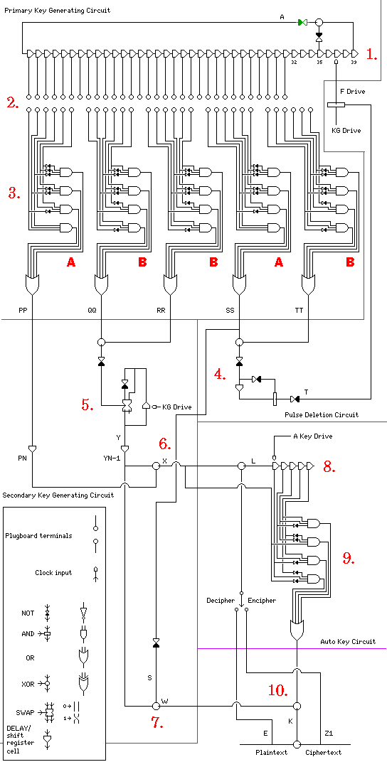
A diagram of the inner workings of the KW-7 follows:
There may be some inaccuracies in what follows, as there were some points not entirely clear to me, but at least my description should give the basic level of complexity of the cipher.
The KW-7 functions as a telecipher machine, so the plaintext on which it operates consists of teletypwriter characters, consisting of a start bit of zero, five data bits, and a stop bit of one. With teletypewriters, the stop bit may take a longer time than the other bits; with 5-level code, a stop bit taking 1.5 times as long as other bits is common; with 8-level code, one can use either one or two stop bits. Since the KW-7 buffers one character internally, it is important to ensure it doesn't output characters too rapidly for the equipment at the other end. Thus, it has a setting for either one stop bit, or for 1.42 stop bits as the minimum in what it outputs.
The diagram only shows the portions of the machine relevant to its cryptographic algorithm; it also contains, for example, much circuitry for the purpose of synchronizing with the input stream of teletypewriter characters.
Theoretically, a machine of this type could be designed to work with 8-level or 6-level codes as well, although this would change the cipher because some parts of the machine are clocked only for the data bits, and others are clocked for the start and stop bits, but this was not done with the KW-7. Which was no doubt wise, as even if the same key was never used for communications with teletypewriters with different numbers of data bits per character, there is still the potential for the comparison of messages of these different kinds to open additional avenues for cryptanalysis by revealing things about the machine's workings that would otherwise be hidden.
This is important to understand, because this affects how the shift registers in the machine are clocked. The primary 39-stage shift register, intended to produce a pseudorandom keystream, is clocked for the start and stop bits of input characters as well as for their data bits (although occasionally its clock may be paused, as we will see below). The 5-stage shift register used for the autokey function, on the other hand, is clocked only for data bits.
The clock signal with a pulse for the start, stop, and each of the data bits is called KG DRIVE, and the clock signal with a pulse for each of the data bits only is called A KEY DRIVE in the source manual.
Also, as I use, for greater legibility in small sizes, among other things, my own set of logic symbols, the diagram includes, on the lower left, an inset that is a key to those symbols.
On the diagram, ten sections of the machine are indicated by numbers, largely following the manner in which it is described in my source.
The Primary Key Generating Circuit includes sections 1, 2, and 3 as I describe them below, except that the XOR between the output of shift register cell 39 and the inverse of the output of shift register cell 35 is instead part of the Fibonacci Feedback Circuit:
Section 1 is the main 39-stage shift register. It appears to be a nonlinear shift register, in that the signal from the 39th and final stage is XORed with the inverse of the output of the 35th stage before being fed back into the beginning of the shift register.
Note that there is an inverter shown in green just after the XOR gate. This is because in another place, an XOR gate is described as producing an inverse output, in such a way as to suggest that this is considered normal. So I put one here in a light color to indicate that the output of this XOR gate (and indeed all others shown without an explicit inverter following) may be inverted.
Thus, I'm not sure this is a nonlinear shift register, as that impression may be confusion on my part due to the device using negative logic, leading to my having been confused by the description.
If I am mistaken in having the feedback bit inverted, it is also of interest that 1 + x^4 + x^39 is a primitive polynomial over the Galois Field of 2. As noted on the first page of this section, the reversal property for primitive polynomials reverses things around a point just a bit earlier than the center of the shift register, so a tap on the fourth stage from the left can be replaced by a tap on the fifth stage from the right (which makes sense because the reversal shouldn't include the always-tapped final stage). Thus, if that inversion isn't supposed to be there, then it is using an LSFR based on a primitive polynomial and therefore with maximum period.
Also, it may be noted that if the inverter shown in green is present, since inverting one of the inputs to an XOR always inverts the output, that would be equivalent to both inverters being absent. Thus, the explicit statement that the signal from stage 35 is inverted before being fed to the XOR circuit, if the XOR circuit actually produces a not XOR signal, would not prevent the main shift register from being an LFSR.
Examining the schematic for enlightenment on this point suggests that this may be what is taking place, but I cannot claim to be completely sure.
Section 2 is shown as a plugboard. Actually, it does not involve patch cords, but instead there is a connector into which a key module is inserted that makes the connections in a particular jumbled manner.
What is connected are 30 of the first 31 stages of the shift register to the six inputs of five combiner circuits. Originally, I misunderstood the way in which this was phrased, so that I thought that only 30 of those stages were available for connection, but in fact all 31 are available for use, so which one is omitted is also part of the key.
Section 3 is the five combiner circuits. These produce signals which I refer to as PP, QQ, RR, SS, and TT. In the original source, they were not p, not q, not r, not s, and not t respectively. I chose doubled letters for two reasons: capital letters are more legible in these diagrams the way I'm drawing them, and as there is another signal named T, having signals t and T is asking for confusion.
The combiner circuits come in two types, labelled A and B in the diagram.
It could be considered a slight imperfection of this device that both of the combiner circuits, the outputs of which are XORed together to form the signal controlling the Accumulator, are of type B; thus, the inputs to the combiners forming the QQ and RR signals could be switched to make an equivalent key. While SS and TT are also XORed together, the SS signal by itself is also used somewhere else, and yet the combiners forming those two signals are different. However, this is a very minor imperfection.
The two types of combiner circuits in this section, and the similar combiner circuit of a third type in section 9, share important common characteristics.
The output is an OR of four ANDs, and each AND combines three inputs from the main shift register. As the inputs are pseudo-random, they have each a probability of about 0.5 of being a 1. (The period of an LFSR is a large odd number, so that probability is actually very slightly larger than 0.5, since the all-zeroes state is not allowed.) So the probability of the output of each of the AND gates being a 1 would also be very close to 0.125 or 1/8, since the three inputs derive from three different bits.
If these AND gates produced completely independent outputs, though, then instead of the probability of their OR being a 1 being close to 0.5, it would be around 0.4138..., or 1 minus (7/8)^4.
But the AND gates are not independent of each other.
Instead, they are arranged in a fashion that has some symmetries.
Each of the six input signals to a combiner is a direct input to one of the AND gates, and is input in inverted form to another one of the four AND gates. So those two AND gates cannot both output a 1 at the same time, as only one of these two signals will be a 1 at any given time.
And "4 choose 2" (the number of ways two different objects can be chosen from a set of four, which is (2! * 2!)/4!) happens to be six.
Let us look at the arrangements of the three kinds of combiner:
Type A

 1   2   3
~1           4       6
    ~2      ~4   5
        ~3      ~5  ~6


Type B

~1   2   3
 1           4      ~6
    ~2      ~4   5
        ~3      ~5   6


Section 9

~1   2          ~5
    ~2   3           6
 1          ~4      ~6
        ~3   4   5
Each row in the chart above lists the three inputs to one of the four AND gates for a given combiner, and these inputs are organized so that inputs from the same source are in the same column.
As can be seen by inspection, for each of the three inputs to one of the AND gates, the complements of those inputs are always split among all three of the other AND gates.
Therefore, no two of the AND gates will ever produce a 1 at the same time, and so the chance of a 1 as the output from the final OR of their four outputs is not reduced by overlap.
The Pulse Deletion Circuit includes section 4, as I describe it below, and some additional circuitry not included in the diagram for simplicity:
Section 4 is where a gating signal used to pause the stepping of the main shift register is generated. Signals SS and TT are XORed with the result inverted. The stream of bits goes through a delay, allowing logic to produce a signal that is a 1 only if the current bit in the stream is 0, but the previous one was 1.
The inverse of that result is used to gate the clock pulses which advance the main shift register.
Since if the current bit is 0, at the next clock time the previous bit cannot be 0, the shift register can't be paused for two clock times in a row. (So the delay or flip-flop in this section is clocked for the start bit, the data bits, and the stop bit, this clock also being the input to the AND gate where the clock for the main shift register is gated. No attempt is made to show clocking in the diagram, to avoid excessive complexity. Alarm circuitry to indicate if the shift register generates too many zeroes in a row, or to detect other error conditions, are also neither illustrated nor discussed here.)
The Secondary Key Generating Circuit includes sections 5, 6, and 7 as I describe them below:
Section 5 is where signals QQ and RR are merged by an XOR, inverted, and then the result is fed to a circuit called an Accumulator.
The Accumulator normally produces an alternating sequence of 0 and 1 bits, but when the input is a 1, the next bit is the same as the preceding bit instead.
The output of the Accumulator is delayed by one clock time, before being used below.
It appears to me that the Accumulator plays a vital role in the cryptographic security of the KW-7. As we've seen in the discusson of the previous section of the device, the primary 38-stage shift register sometimes has a clock pulse deleted. This creates an irregularity in the bitstream that it outputs, which is a good thing. But it also means that the bitstream it outputs has an elevated probability that any given bit will be followed by another bit with the same value.
The Accumulator produces a bitstream that doesn't have deleted clock pulses. Because it alternates from 0 to 1, except when an input bit, which has a probability close to 1/2 of being a 1, is 1, each bit in that output bitstream has a probability of about 0.5 of being different from the previous bit, like the bits in a truly random stream of bits.
Thus, when the output from the Accumulator is XORed together with an output taken from the primary shift register, the benefits of making it irregular by pausing the clock are retained, but the fact that the clock is paused is no longer visible.
Of course, there are other more direct ways of dealing with this. One of the most obvious would be to have a second primary shift register, which also has its clock pulses deleted on occasion, but never at the same time as thos of the first primary shift register.
Another would be to occasionally send two clock pulses, instead of one, to the primary shift register, instead of deleting the clock pulse.
However, because the KW-7 was already a big and bulky piece of equipment, given the technology of its day, the first alternative would not have been practical, and while electronics could easily outpace the speed of teletypewriter signals, the second alternative would no doubt also have involved more complexity than the one chosen.
The fact that this machine takes a single shift register, and modifies its sequence to make it cryptosecure through two very simple modifications, deleting occasional clock pulses, and creating an additional signal from the Accumulator to mask that, suggests that the KW-7 design approaches the absolute minimum in complexity for a cryptosecure stream cipher device.
Section 6 shows a couple of XOR gates that play an important role in connecting together the major sections of the device and completing the process of encipherment.
First, the PP combiner output, after a single-clock delay, (called the PN signal) is XORed with the delayed Accumulator output. This produces a signal called X. Then this signal is XORed with the delayed ciphertext output to produce the signal called L which is the input to the autokey shift register.
Section 7 is an XOR involving the delayed Accumulator output, which is used as the primary keystream. It is XORed with a signal called S, which is the inverse of the signal I had designated as SS (instead of not s) in my diagram. The description seemed to suggest that it was a clock signal instead, which did not make sense to me, but as the manual that was my source also included schematics, I was able to resolve the issue from them.
The Auto Key Circuit includes sections 8 and 9 as I describe them below:
Section 8 consists of an XOR between signal X (which is itself the XOR of the delayed Accumulator output YN-1 and the delayed PP signal, PN, as we saw in the description of Section 6) with the ciphertext stream, and the autokey shift register. This is a five-stage shift register without feedback. As noted above, it is clocked for the data bits, and not the start and stop bits, of the teletypewriter characters being enciphered.
When the machine is enciphering plaintext, the ciphertext stream is the final output of the machine; when it is deciphering ciphertext, the ciphertext stream is instead the input to the final key addition. A switch to select between these two possibilities is now shown in the diagram.
Section 9 is the combiner which produces the autokey keystream. It has the same general design as the five combiners used with the primary 39-stage shift register. The six signals it combines are the signal designated X, which is not affected by the ciphertext, but is produced by the keystream generator circuitry only, and the outputs of the five shift register stages, which are all bits in the sequence of L bits, which do involve the ciphertext.
The Final Key Generating and Key Adding Circuit corresponds to Section 10 as I describe it below:
Section 10 consists of the XOR between the main keystream, the signal W from Section 10, with the output of the Autokey circuitry; this XOR is followed by the XOR which applies the full keystream to the plaintext to produce cipher.
As I noted above, the Accumulator makes up for the fact that irregularity in the output of the primary shift register is provided by stopping it from moving on occasional clock cycles.
Also, when I noted this, I pointed out that the "obvious" way to address this issue would have been, instead, to add a second shift register to the design.
An additional shift register would still be a very good thing to add once it became possible through the use of more advanced and compact electronic technology.
Thus, this diagram illustrates one way the design could have been extended from its original form:
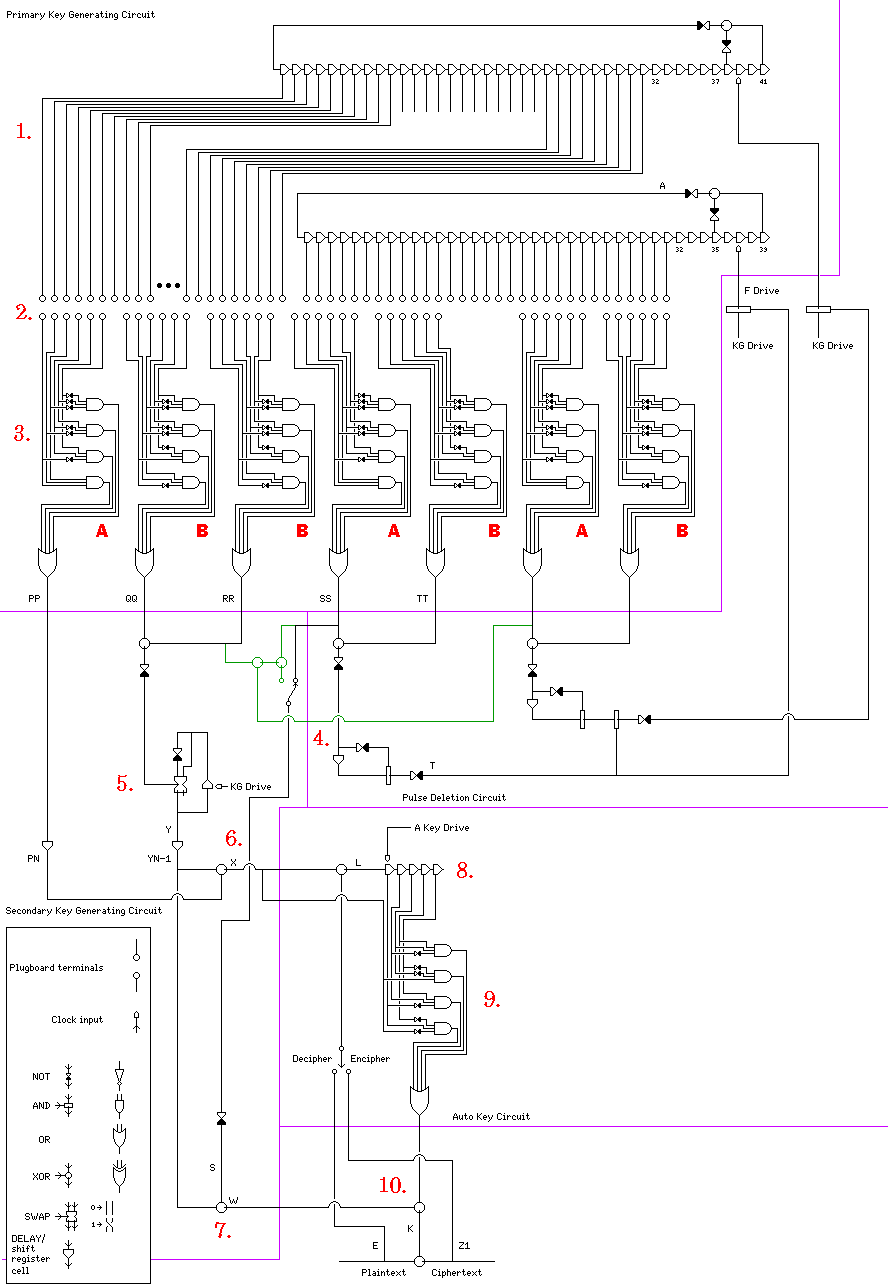
A nice primitive polynomial is available in trinomial form for a shift register two stages longer than the one originally used, and so the additional shift register is 41 stages in length, instead of 39, and the feedback tap is moved accordingly.
Note that the inverter after the XOR is no longer in green; in this design, the shift registers are definitely LFSRs, not non-linear.
Two additional combiners are added, and the XOR of their outputs also produces a signal to inhibit clocking, this time of the second shift register, when there is a 1 followed by a zero in their output sequence. But in addition, this inhibition signal is removed whenever the first shift register is not clocked.
The first thirty-one stages of the second shift register are added to the first thirty-one stages of the first shift register as possible inputs to the combiners; since there are seven of them instead of five, they require 42 input signals instead of 30, so now 42 signals are chosen from 62 instead of 30 signals being chosen from 31.
If these additions were the only changes, it would be possible to provide a successor to the KW-7 designed this way with the ability to also interoperate with the original KW-7.
One additional possible change is shown in green: with a switch, so as to preserve interoperability, both the RR signal, and one of the two combiner outputs used to produce the clock inhibit bit for the second shift register, can be XORed with the SS signal before its complement is XORed with the Accumulator output to form the W signal.
This addresses the issue of both combiners being used to form the input to the accumulator being of the same type, and makes the W signal more complex.
Another possible change, not shown in the diagram, would be to derive the clock for the second shift register from A KEY DRIVE instead of KG DRIVE. Having the shift register in the primary key generation circuit clocked on the start and stop bits as well as the data bits is a nice wrinkle, but with two shift registers, it isn't necessary to do it for both of them, and not doing it for the second shift register adds to the differences between the two and thus the uniqueness of each.
While I have to admit that despite admiring the ingenuity of the design of the original KW-7, I was concerned that it might be lacking in security as a result of relying on one shift register, despite all its other features. Because the inputs to each combiner can be taken from both of the two shift registers, one of which is always moving, and which have relatively-prime periods, superficially, at least, this seems much more secure, despite the fact that LFSRs are dangerously weak as a result of being linear, and the linearity even in this apparently more complex design is still only thinly masked.
2^39-1 is 7 * 79 * 8191 * 121369, and 2^41-1 is 13367 * 164511353, so they are indeed relatively prime despite the fact that 2^41-1 is not prime.
Adding a second shift register, though, adds a lot of extra circuitry to the device. Could it be made more secure in a simple way, not involving more than a minimal amount of extra circuitry?
As I noted, electronic logic is capable of operating at a speed much faster than the baud rate of teletypewriter signals. While the A KEY DRIVE signal needs to be left alone, as the autokey function needs to work on new ciphertext bits at each step, a circuit could be added that generates additional pulses in the KG DRIVE signal, doubling its clock rate. In addition, so as to provide greater nonlinearity, these additional bits only, before being combined with the original clock pulses of the KG DRIVE signal, could go through an AND gate with the RR signal as its other input. So the rate of clock pulses would be doubled, but only half the time. An additional circuit would also be needed to gate and buffer the keystream output in the W signal before XORing it with the signal from the Auto Key section, so that doubling the clock rate of the key generator doesn't cause the output enciphered signal to change state in the middle of a bit time. Of course, in a cipher machine, gating and buffering is required in any case, so that the output signal doesn't reveal information because the keystream changes state slightly before or after the plaintext signal advances to the next serial bit, and so the time chosen for the clock pulses that regulate that can be chosen to deal with this issue as well (for example, those clock pulses could be placed halfway between the regular KG DRIVE pulses and the additional pulses that follow them).
However, this apparently simple change will interact badly with one aspect of the device: the existing deletion of 1/4 of the clock pulses at random, but never two in a row. Now that this part of the cipher machine is operating twice as fast, one could have two consecutive regular pulses deleted, and the additional pulse between them also deleted, in the design just described.
Next
Chapter Start
Skip to Next Chapter
Table of Contents
Home Page