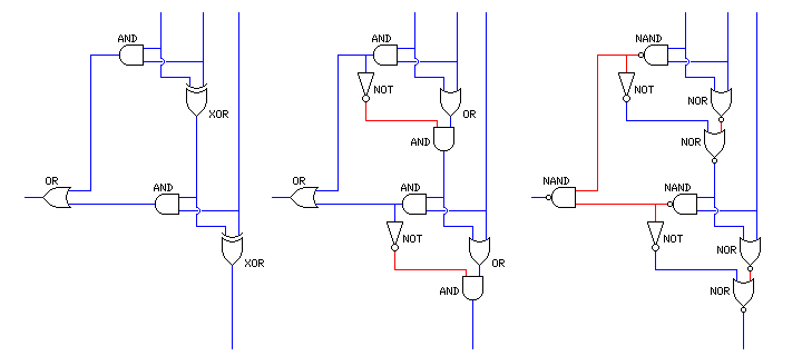
This diagram shows three possible depictions of the design of a full adder.
On the left is the most common diagram, showing how a full adder is composed of two half adders, each one using an AND gate to obtain the carry, and an XOR gate to obtain the sum.
The middle diagram shows how the XOR gate, which usually cannot be built directly in most logic families, can be replaced so that the design uses only the elementary AND, OR, and NOT logic gates.
The diagram on the right shows how the full adder is transformed when some of its internal signals are inverted, through the use of NAND and NOR gates, instead of AND and OR gates, as some forms of logic, such as both TTL and CMOS, provide. Note that since a NAND gate may be thought of either as an AND gate with its output inverted, or an OR gate with both of its inputs inverted, and similarly a NOR gate may be thought of either as an OR gate with its output inverted, or an AND gate with both of its inputs inverted, in some cases OR gates are replaced by NAND gates, and AND gates are replaced by NOR gates.
In order that this transformation process is clear, lines showing inverted signals are shown in red, while lines showing conventional signals are shown in blue.
We need to get our feet wet somewhere, to begin expressing the design of our example computer. Hence, here is how the design of one of its most basic elements, the full adder, could be described:
// Full Adder cell
module fa( c_out, sum, a1, a2, c_in );
// port declaration division
 input  a1, a2, c_in ;
 output c_out, sum ;
// variable declaration division
 wire   c_out, sum, a1, a2, c_in ;
 wire   haci_1, hac_1, hati_1, has_1, haci_2, hac_2, hati_2 ;
// procedure division
 nand #1 ( haci_1, a1, a2 ) ;
 nor  #1 ( hati_1, a1, a2 ) ;
 not  #1 ( hac_1,  haci_1 ) ;
 nor  #1 ( has_1,  hac_1, hati_1 ) ;
 nand #1 ( haci_2, has_1, c_in ) ;
 nand #1 ( c_out,  haci_1, haci_2 ) ;
 nor  #1 ( hati_2, has_1, c_in ) ;
 not  #1 ( hac_2,  haci_2 ) ;
 nor  #1 ( sum,    hac_2, hati_2 ) ;
endmodule
This is an example of code in the Verilog language, in this case at the gate level.
As in C++, two slashes are used to indicate a comment.
The inputs and outputs of the module are declared following the line with the header prototype.
Variables which represent the propagation of a logical signal are declared to be of type wire.
As in C, statements are terminated with semicolons.
The nand and nor gates are predefined as subroutines. The notation #1 indicates for purposes of simulating the circuit described that the gates shown are to be considered to have an intrinsic delay of one.
The Verilog language allows constructs to be described in more than one way. It is also possible to describe a full adder at the Register Transfer Level:
// Full Adder cell
module fa( c_out, sum, a1, a2, c_in );
// port declaration division
 input  a1, a2, c_in ;
 output c_out, sum ;
// variable declaration division
 wire   c_out, sum, a1, a2, c_in ;
// procedure division
 { c_out, sum } = #(2:4:5) a1 + a2 + c_in ;
endmodule
This explains the function of the full adder in terms of what it is supposed to do, rather than in terms of what it is made of.
Listing items within braces performs concatenation; note that concatenated objects are permitted on the left-hand side of an assignment.
A delay, in this case specifying minimum, typical, and maximum values for the delay is still included. While it would not be necessary in an idealized description of a full adder cell, if the RTL version of the module is compared to the gate level version, obviously we don't want the gate level version to fail the comparison because it has delays, while the target against which it is tested does not.