Welcome to the home page of the Concertina III computer architecture.
After a very long period of basic design, I finally achieved my goals of code compactness with the Concertina II architecture. However, stepping back and looking at it dispassionately, it was clear to me that even with "only" eight types of block headers, which was considerably less than I had in some iterations of the design, it was still far too complicated to have any chance of widespread adoption.
Also, I finally came to the realization that since instruction fetch and decode can be performed well in advance of instruction execution, avoiding sequentiality in decoding by making all instructions the same length, unless a header explicitly indicates where they begin, has no real benefit.
Not too long ago, I had made one attempt to transition to Concertina III, but it seemed as though there was not enough opcode space to provide the type of instruction set I wanted without headers and only with variable-length instructions, after making the sacrifice of going to register banks of sixteen registers instead of thirty-two. However, taking another look, and making another attempt, it seems as though this is not the case.
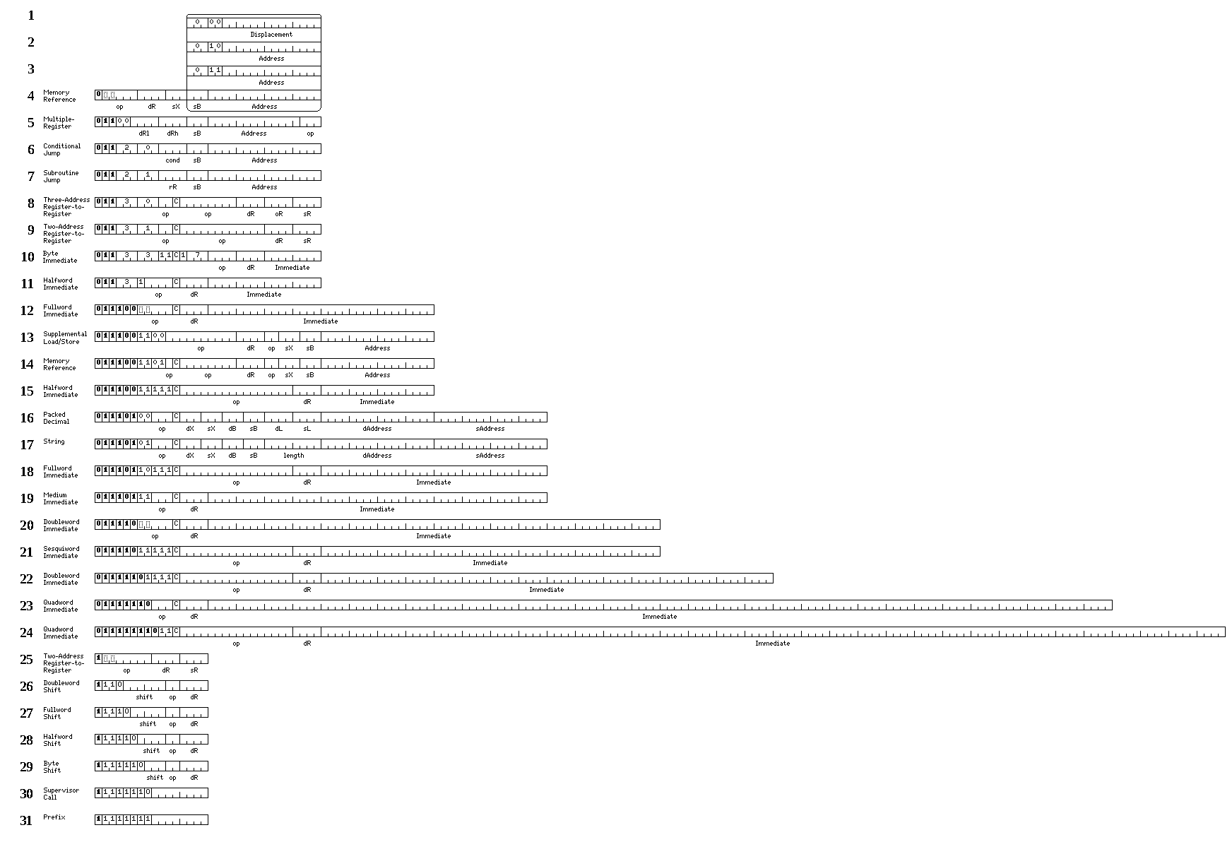
This diagram illustrates the basic instruction formats of Concertina III:
16-bit instructions consume fully half the opcode space. Only operate instructions, shift instructions, and the Supervisor Call instruction are provided at that length.
32-bit instructions are allocated 7/16ths of the opcode space. This appears to be sufficient to include even such problematic instructions as multiple-register load and store instructions, and halfword immediate instructions, among the 32-bit instructions.
In order that the instructions can fit into the opcode space, a basic feature of the Concertina II architecture has been taken over in a simplified form.
Only integer registers 1 to 7 may serve as index registers, and only integer registers 9 to 15 may serve as base registers.
The first four lines of the diagram show the available addressing modes for normal memory-reference instructions. Line 4 shows normal base-index addressing; the previous three lines show the additional addressing modes made available when the base register field contains all zeroes.
In Line 1, we see relative addressing, where the Displacement field contains a signed relative displacement in bytes. The value of zero points to the address immediately following the instruction.
In Line 2, we see Array Mode. Here, the Address field is shifted left three positions, and added to the contents of integer register 8 to form an address. The 64-bit integer value at that location, possibly with the value of an index register added to it, if indexing is specified for the instruction, forms the effective address of the instruction itself.
The intent is to allow the use of a table in memory containing the start addresses of multiple large arrays to enable the use of arrays larger than 64K bytes in size without allocating a base register to each one, or requiring additional setup instructions for array accesses.
In line 3, the Address field is again shifted left three positions, and added to the contents of integer register 8; but now it is the sum which, possibly with the value of an index register added to it, if indexing is specified for the instruction, that forms the effective address of the instruction.
This addressing mode is intended to facilitate loading the table of array addresses without placing its location both in integer register 8 and also in one of the base registers.
Line 31 shows the format of a 16-bit instruction prefix which allows the instruction set to be extended. What follows a prefix need not be a regular instruction, modified only in meaning; a prefix may indicate that what follows is an instruction the length of which is decoded in a different manner.